5 pwm output port control, Pwm output port control, Table 12-6 – Freescale Semiconductor MC68HC908MR32 User Manual
Page 135
Output Control
MC68HC908MR32 • MC68HC908MR16 Data Sheet, Rev. 6.1
Freescale Semiconductor
135
12.5.5 PWM Output Port Control
Conditions may arise in which the PWM pins need to be individually controlled. This is made possible by
the PWM output control register (PWMOUT) shown in
.
If the OUTCTL bit is set, the PWM pins can be controlled by the OUTx bits. These bits behave according
to
.
When OUTCTL is set, the polarity options TOPPOL and BOTPOL will still affect the outputs. In addition,
if complementary operation is in use, the PWM pairs will not be allowed to be active simultaneously, and
dead-time will still not be violated. When OUTCTL is set and complementary operation is in use, the odd
OUTx bits are inputs to the dead-time generators as shown in
. Dead-time is inserted
whenever the odd OUTx bit toggles as shown in
. Although dead-time is not inserted when
the even OUTx bits change, there will be no dead-time violation as shown in
Setting the OUTCTL bit does not disable the PWM generator and current sensing circuitry. They continue
to run, but are no longer controlling the output pins. In addition, OUTCTL will control the PWM pins even
when PWMEN = 0. When OUTCTL is cleared, the outputs of the PWM generator become the inputs to
the dead-time and output circuitry at the beginning of the next PWM cycle.
NOTE
To avoid an unexpected dead-time occurrence, it is recommended that the
OUTx bits be cleared prior to entering and prior to exiting individual PWM
output control mode.
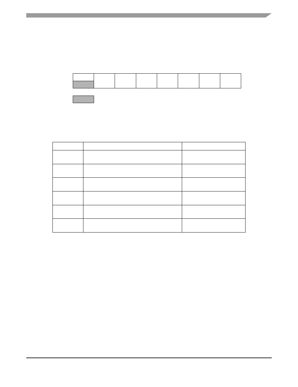
Address:
$0025
Bit 7
6
5
4
3
2
1
Bit 0
Read:
0
OUTCTL
OUT6
OUT5
OUT4
OUT3
OUT2
OUT1
Write:
Reset:
0
0
0
0
0
0
0
0
= Unimplemented
Figure 12-22. PWM Output Control Register (PWMOUT)
Table 12-6. OUTx Bits
OUTx Bit
Complementary Mode
Independent Mode
OUT1
1 — PWM1 is active.
0 — PWM1 is inactive.
1 — PWM1 is active.
0 — PWM1 is inactive.
OUT2
1 — PWM2 is complement of PWM 1.
0 — PWM2 is inactive.
1 — PWM2 is active.
0 — PWM2 is inactive.
OUT3
1 — PWM3 is active.
0 — PWM3 is inactive.
1 — PWM3 is active.
0 — PWM3 is inactive.
OUT4
1 — PWM4 is complement of PWM 3.
0 — PWM4 is inactive.
1 — PWM4 is active.
0 — PWM4 is inactive.
OUT5
1 — PWM5 is active.
0 — PWM5 is inactive.
1 — PWM5 is active.
0 — PWM5 is inactive.
OUT6
1 — PWM 6 is complement of PWM 5.
0 — PWM6 is inactive.
1 — PWM6 is active.
0 — PWM6 is inactive.