Ions in, Figure 19-1, Figure 19-1. spi master timing – Freescale Semiconductor MC68HC908MR32 User Manual
Page 270
Electrical Specifications
MC68HC908MR32 • MC68HC908MR16 Data Sheet, Rev. 6.1
270
Freescale Semiconductor
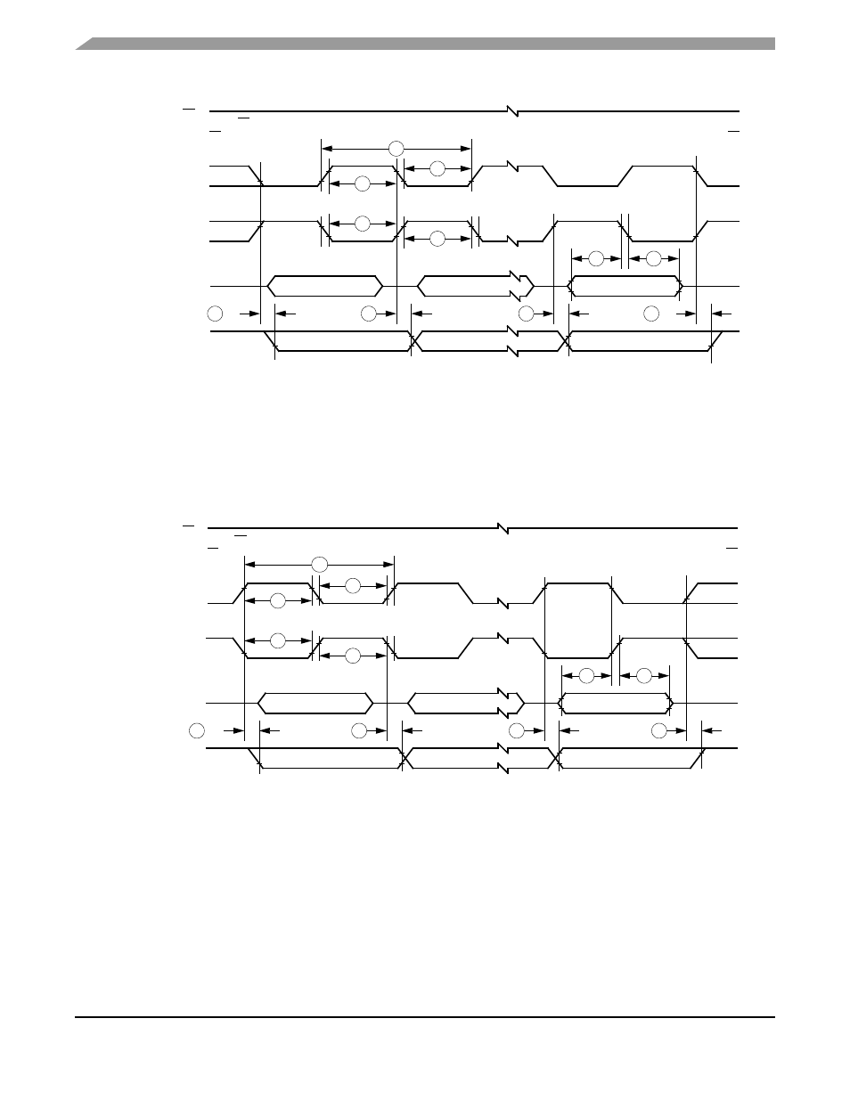
Figure 19-1. SPI Master Timing
NOTE
SS PIN OF MASTER HELD HIGH
MSB IN
SS
INPUT
SPCK, CPOL = 0
OUTPUT
SPCK, CPOL = 1
OUTPUT
MISO
INPUT
MOSI
OUTPUT
NOTE
4
5
5
1
4
BITS 6–1
LSB IN
MASTER MSB OUT
BITS 6–1
MASTER LSB OUT
10
11
10
11
7
6
NOTE
Note: This last clock edge is generated internally, but is not seen at the SCK pin.
SS PIN OF MASTER HELD HIGH
MSB IN
SS
INPUT
SPCK, CPOL = 0
OUTPUT
SPCK, CPOL = 1
OUTPUT
MISO
INPUT
MOSI
OUTPUT
NOTE
4
5
5
1
4
BITS 6–1
LSB IN
MASTER MSB OUT
BITS 6–1
MASTER LSB OUT
10
11
10
11
7
6
a) SPI Master Timing (CPHA = 0)
b) SPI Master Timing (CPHA = 1)
Note: This first clock edge is generated internally, but is not seen at the SCK pin.
This manual is related to the following products: