2 rgmii example schematic, 3 rgmii rx timing options, 1 rx_clk delay in phy – BECKHOFF EtherCAT IP Core for Altera FPGAs v3.0.10 User Manual
Page 97: 2 rx_clk delay on pcb, 3 rx_clk delay in fpga with pll, 4 rx_clk delay in fpga without pll, 4 rgmii tx timing options, Rgmii example schematic, Rgmii rx timing options, Rgmii tx timing options
Ethernet Interface
Slave Controller
– IP Core for Altera FPGAs
III-85
9.4.2
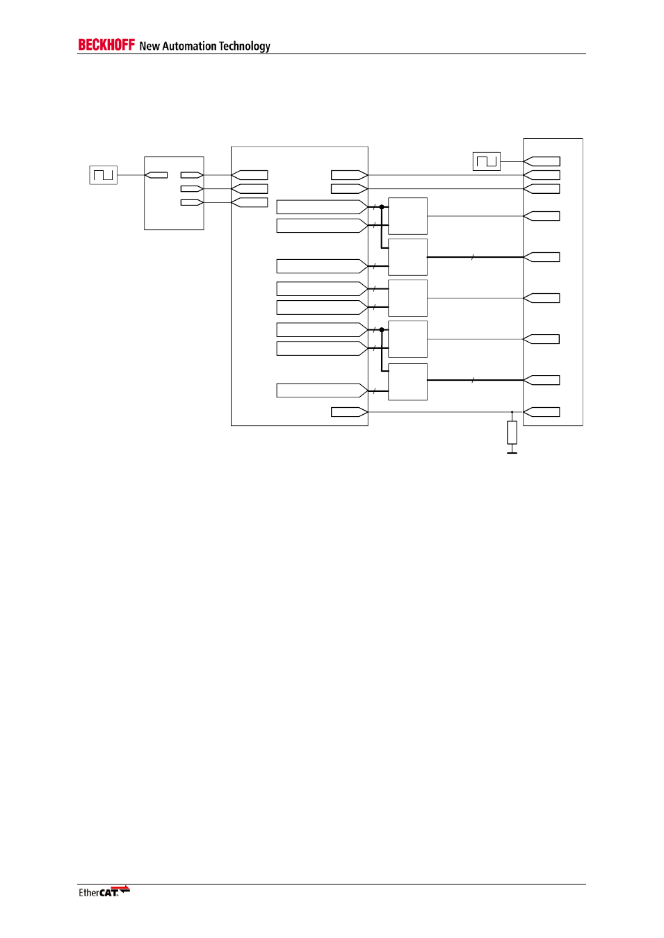
RGMII example schematic
Refer to chapter 8.5 for more information on special markings (!). Take care of proper PHY address
configuration.
EtherCAT IP Core
Ethernet PHY
RGMII_RX_CTL_DATA_DDR_CLK
RGMII_RX_CTL_DATA_DDR_NRESET
RGMII_RX_CLK
RX_CTL
RXD[3:0]
TX_CLK
RX_CLK
REF_CLK
TXD[3:0]
TX_CTL
nMII_LINK
LINK_STATUS
!
CLK25
PLL
CLK_IN
CLK25
CLK100
CLK100
25 MHz
NPHY_RESET_OUT
NRESET
4
K
7
REF_CLK
CLK25_2NS
CLK25_2NS
DDR
input cell
RGMII_RX_CTL_DDR_H
RGMII_RX_CTL_DDR_L
RGMII_RX_DATA_DDR_H[3:0]
RGMII_RX_DATA_DDR_L[3:0]
DDR
input cell
DDR
output
cell
DDR
output
cell
DDR
output
cell
RGMII_TX_CLK_DDR_CLK
RGMII_TX_CLK_DDR_NRESET
RGMII_TX_CLK_DDR_H
RGMII_TX_CLK_DDR_L
RGMII_TX_CTL_DATA_DDR_CLK
RGMII_TX_CTL_DATA_DDR_NRESET
RGMII_TX_CTL_DDR_H
RGMII_TX_CTL_DDR_L
RGMII_RX_DATA_DDR_H[3:0]
RGMII_RX_DATA_DDR_L[3:0]
Figure 32: RGMII example schematic
9.4.3
RGMII RX timing options
RGMII uses a source synchronous interface for receive signals. Originally, RX_CLK and
RX_CTL/RX_DATA are edge-aligned at the PHY side. RX_CLK needs to be delayed to maintain
setup/hold timing at the FPGA side. There are several options for delaying RX_CLK:
9.4.3.1
RX_CLK Delay in PHY
Some PHYs offer RGMII-ID, which means, the RX_CLK is delayed internally in the PHY. The
EtherCAT IP Core itself cannot enable this feature using the MII management interface if the PHY
requires this. It is up to the IP Core user to enable this feature.
9.4.3.2
RX_CLK Delay on PCB
One option is to delay RX_CLK on the PCB.
9.4.3.3
RX_CLK Delay in FPGA with PLL
The delay of RX_CLK can be realized with a PLL at each RGMII port, configured for clock phase shift.
9.4.3.4
RX_CLK Delay in FPGA without PLL
The delay of RX_CLK can be realized with routing delay inside the FPGA.
9.4.4
RGMII TX timing options
RGMII uses a source synchronous interface for receive signals. Originally, TX_CLK and
TX_CTL/RX_DATA are edge-aligned at the FPGA side. TX_CLK needs to be delayed to maintain
setup/hold timing at the PHY side. There are several options for delaying TX_CLK: