Cs bhe wr rd data busy, Internal state – BECKHOFF EtherCAT IP Core for Altera FPGAs v3.0.10 User Manual
Page 123
PDI Description
Slave Controller
– IP Core for Altera FPGAs
III-111
BHE1
CS
BHE
WR
RD
DATA
BUSY
ADR1
ADR
t
WR_active
t
CS_delay
t
WR_delay
t
ADR_BHE_DATA_hold
DATA1
t
ADR_BHE_DATA_setup
t
CS_to_BUSY
(with preceding write access)
t
WR_to_BUSY
t
write
t
CS_to_BUSY
t
CS_to_BUSY
t
BUSY_to_WR_CS
Internal
state
Writing ADR1
Idle
Idle
t
CS_WR_overlap
t
write_int
Writing ADR2
t
write
BHE2
ADR2
DATA2
t
BUSY_to_WR_CS
t
CS_WR_overlap
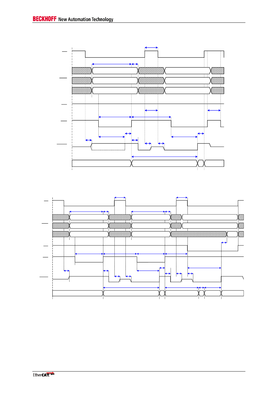
Figure 50: Write access (write after rising edge nWR, without preceding write access)
BHE1
CS
BHE
WR
RD
DATA
BUSY
ADR1
ADR
t
WR_active
t
WR_to_BUSY
t
CS_delay
t
WR_delay
t
ADR_BHE_DATA_hold
DATA1
t
ADR_BHE_DATA_setup
t
write_int
t
CS_to_BUSY
t
CS_to_BUSY
t
CS_to_BUSY
Internal
state
Writing ADR1
BHE2
ADR2
t
WR_active
t
WR_to_BUSY
t
BUSY_to_WR
t
CS_delay
t
ADR_BHE_DATA_hold
DATA2
t
ADR_BHE_DATA_setup
t
read
ADR3
BHE3
t
CS_to_BUSY
t
CS_to_BUSY
Idle
Writing ADR2
Reading ADR3
DATA3
Idle
Idle
t
write
t
write_int
t
WR_to_RD
t
read_int
t
BUSY_to_DATA_valid
Coll.
t
coll
Figure 51: Sequence of two write accesses and a read access
Note: The first write access to ADR1 is performed after the first rising edge of WR. After that, the ESC is internally
busy writing to ADR1. After CS is deasserted, BUSY is not driven any more, nevertheless, the ESC is still writing
to ADR1.
Hence, the second write access to ADR2 is delayed because the write access to ADR1 has to be completed first.
So, the second rising edge of WR must not occur before BUSY is gone. After the second rising edge of WR, the
ESC is busy writing to ADR2. This is reflected with the BUSY signal as long as CS is asserted.
The third access in this example is a read access. The ESC is still busy writing to ADR2 while the falling edge of
RD occurs. In this case, the write access to ADR2 is finished first, and afterwards, the read access to ADR3 is
performed. The ESC signals BUSY during both write and read access.