10 flash memory, Table 7-6, Flash options – Artesyn MVME3100 Single Board Computer Installation and Use (June 2014) User Manual
Page 133: Flash memory, Programming details
Programming Details
MVME3100 Single Board Computer Installation and Use (6806800M28E)
133
7.10 Flash Memory
The MVME3100 is designed to provide one or two physical banks of soldered-on Flash
memory. Each bank may be populated with two AMD Spansion MirrorBit 3.0V devices
configured to operate in 16-bit mode to form a 32-bit Flash bank. The Flash bank connected to
LBC Chip Select 0 is the boot bank and is always populated. The second Flash bank connected
to LBC Chip Select 1 may or may not be populated depending on Flash size requirements and
available Flash devices. The VPD Flash packet(s) will determine which banks are populated and
the size of the devices. Software must program one or two LBC chip selects based on the VPD
Flash packet information. The following table defines the supported Flash density options for
each bank. The factory configuration for the MVME3100-1152 is one bank of 64MB; for the
MVME3100-1263, it is one bank of 128MB.
A hardware Flash bank write protect switch is provided on the MVME3100 to enable write
protection of both physical banks. Regardless of the state of the software Flash write protect
bit in the Flash Control/Status register, write protection is enabled for both banks when this
switch is ON. When this switch is OFF, write protection is controlled by the state of the software
Flash write protect bit and can only be disabled by clearing this bit in the Flash Control/Status
register. Refer to
for more information.
The F_WE_HW bit reflects the state of the switch and is only software readable, whereas the
F_WP_SW bit supports both read and write operations.
TSEC2
Gigabit Ethernet port routed to P2
BCM5461S
02
Fast Ethernet
Controller
10/100 Ethernet port routed to P2
BCM5221
03
Table 7-5 PHY Types and MII Management Bus Addresses (continued)
MPC8540
Ethernet Port
Function/Location
PHY Types
PHY MIIM Address
[4:0]
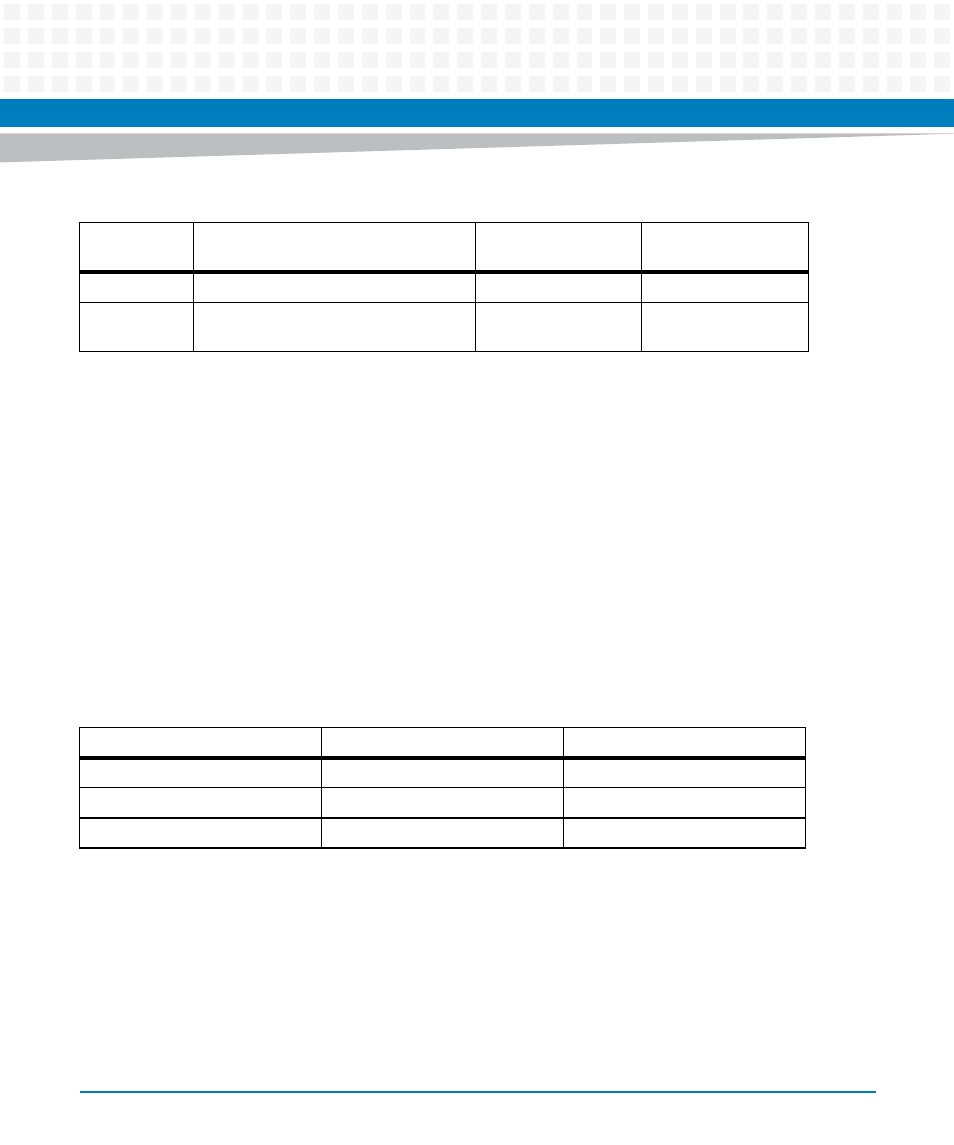
Table 7-6 Flash Options
Flash Bank Size
Spansion Part Number
Device Size
32MB
S29GL128N
128 Mbit
64MB
S29GL256N
256 Mbit
128MB
S29GL512N
512 Mbit