Memory maps, 1 memory maps, 1 default processor memory map – Artesyn MVME3100 Single Board Computer Installation and Use (June 2014) User Manual
Page 105: Table 6-1, Default processor address map, Chapter 6
Chapter 6
MVME3100 Single Board Computer Installation and Use (6806800M28E)
105
Memory Maps
6.1
Memory Maps
6.1.1
Default Processor Memory Map
The MPC8540 presents a default processor memory map following RESET negation. The
following table shows the default memory map from the point of view of the processor. The
e500 core only provides one default TLB entry to access boot code and it allows for accesses
within the highest 4KB of memory. To access the full 8MB of default boot space (and the 1MB
of CCSR space), additional TLB entries must be set up within the e500 core for mapping these
regions. Refer to the MPC8540 Reference Manual listed in
Appendix B, Related Documentation
for details.
This is the default location for the CCSRs, but it is not mapped after reset.
Only FFFF F000 to FFFF FFFF is mapped after reset. The e500 core fetches the first instruction
from FFFF FFFC following a reset.
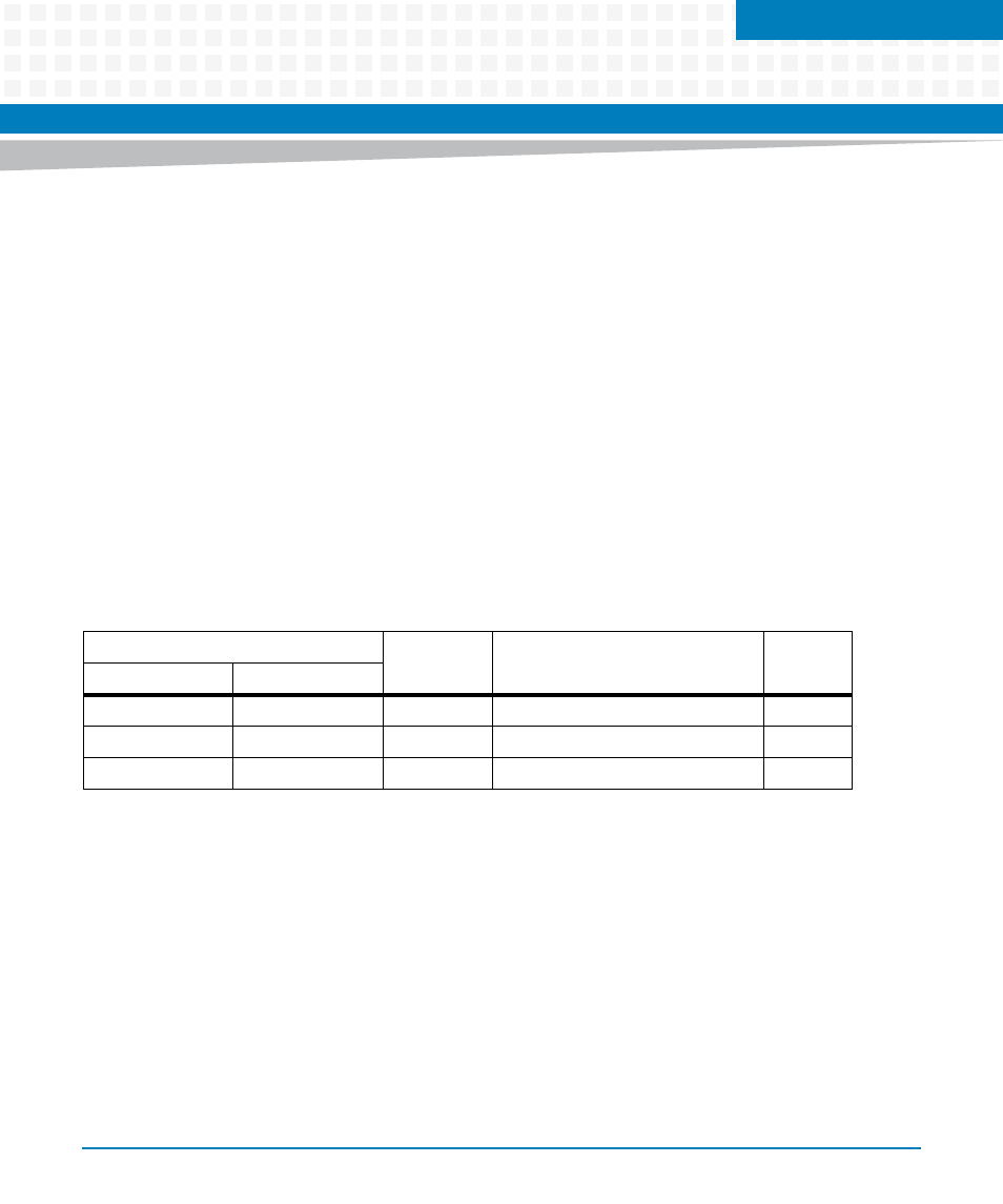
Table 6-1 Default Processor Address Map
Processor Address
Size
Definition
Notes
Start
End
0000 0000
FF6F FFFF
4087M
Not mapped
FF70 0000
FF7F FFFF
1M
MPC8540 CCS Registers
1
FF80 0000
FFFF FFFF
8M
Flash
2
- ARTM-9405 16x10GbE Installation and Use Guide (May 2014) (64 pages)
- ATCA 7370 / ATCA 7370-S Installation and Use (January 2015) (256 pages)
- ATCA 7370 / ATCA 7370-S Installation and Use (September 2014) (254 pages)
- ARTM-831X Installation and Use (June 2014) (346 pages)
- ATCA-7350 - Integrating with Workbench User Guide (September 2014) (34 pages)
- ATCA-7350 Installation and Use (September 2014) (208 pages)
- ATCA-7365-CE Installation and Use (May 2014) (306 pages)
- ATCA-7365-CE Installation and Use (Jan 2015) (300 pages)
- ATCA-7365-CE Installation and Use (May 2014) (294 pages)
- ATCA-7368 Installation and Use (June 2014) (222 pages)
- ATCA-7475 Installation and Use (October 2014) (284 pages)
- ATCA-7480 Installation and Use (April 2015) (330 pages)
- ATCA-8330 Installation and Use (April 2015) (236 pages)
- ATCA-8320 Installation and Use (May 2014) (456 pages)
- ATCA-9305 User's Manual (May 2014) (270 pages)
- ATCA-9405 Installation and Use (October 2014) (168 pages)
- ATCA-F120 Installation and Use (August 2014) (122 pages)
- ATCA-F140 Installation and Use (September 2014) (138 pages)
- ATCA-MF106 Installation and Use (September 2014) (86 pages)
- Centellis-4440/AXP1440 Installation and Use (September 2014) (208 pages)
- Centellis 4410 (AXP-1410) Installation and Use (July 2014) (202 pages)
- Centellis 2100 Release 3.0 Installation and Use (March 2015) (192 pages)
- Centellis 2100 Release 3.0 Installation and Use (March 2015) (176 pages)
- Centellis 2000 User Card-10GE Installation and Use (May 2014) (54 pages)
- Centellis 2000 User Card-10GE with Telco Alarm Installation and Use (May 2014) (60 pages)
- COMX-CAR-210 Installation and Use (August 2014) (76 pages)
- COMX-P1022 Installation and Use (July 2014) (84 pages)
- COMX-P2020 Installation and Use (February 2015) (100 pages)
- COMX-CORE Series Installation and Use (August 2014) (128 pages)
- COMX-P2020 Installation and Use (July 2014) (100 pages)
- COMX-P4080-2G-ENP2 Installation and Use (August 2014) (70 pages)
- COMX-P4080 Installation and Use (August 2014) (126 pages)
- COMX-P40x0 ENP2 Installation and Use (August 2014) (130 pages)
- COMX-P40x0 ENP2 Installation and Use (January 2015) (140 pages)
- iVPX7225 RTM Installation and Use (April 2015) (56 pages)
- MITX-430/MITX-440-DVI-2E Installation and Use (August 2014) (118 pages)
- CPCI-6200 Installation and Use (May 2015) (234 pages)
- SCP-MITX-CORE-820-SM Installation and Use (August 2014) (132 pages)
- iVPX7225 Installation and Use (April 2015) (168 pages)
- MVME2502 Installation and Use (December 2014) (166 pages)
- MVME2502 Installation and Use (August 2014) (150 pages)
- MVME2500 VxWorks 6.8 AMP User Guide (August 2014) (40 pages)
- MVME2500 VxWorks 6.8 User Guide (April 2014) (44 pages)
- MVME4100 Single Board Computer Installation and Use (June 2014) (136 pages)