2 motload’s processor memory map, 3 vme memory map, Table 6-2 – Artesyn MVME3100 Single Board Computer Installation and Use (June 2014) User Manual
Page 106: Motload’s processor address map
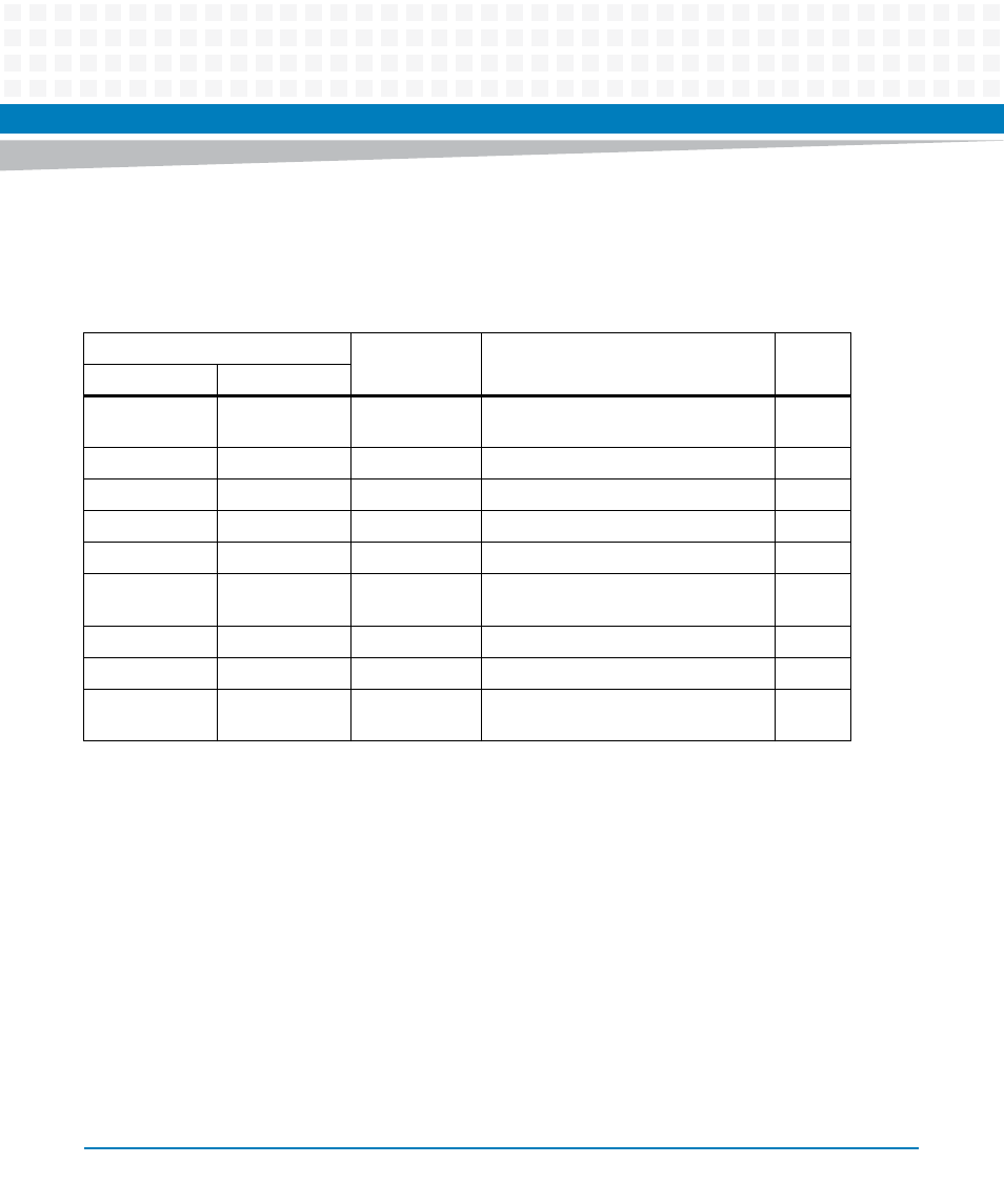
Memory Maps
MVME3100 Single Board Computer Installation and Use (6806800M28E)
106
6.1.2
MOTLoad’s Processor Memory Map
MOTLoad’s processor memory map is given in the following table.
After RESET, the MPC8540 does not map any PCI memory space (inbound or outbound), and
does not respond to Config cycles.
6.1.3
VME Memory Map
The MVME3100 is fully capable of supporting both the PReP and the CHRP VME Memory Map
examples with RAM size limited to 2GB.
Table 6-2 MOTLoad’s Processor Address Map
Processor Address
Size
Definition
Notes
Start
End
0000 0000
top_dram-1
dram_size
(2GB max)
System Memory (on-board DRAM)
8000 0000
DFFF FFFF
1.5GB
PCI Memory Space/VME
E000 0000
E0FF FFFF
16MB
PCI I/O Space
E100 0000
E10F FFFF
1MB
MPC8540 CCSR
E1100 0000
E1FF FFFF
15MB
Not Used
E200 0000
E2FF FFFF
16MB
Status/Control Registers/UARTs,
External Timers
E300 0000
EFFF FFFF
208MB
Not Used
F000 0000
F7FF FFFF
128MB
Reserved
1
,
2
bottom_flash
FFFF FFFF
flash_size
(128MB max)
Flash
2
1. Reserved for future larger flash devices.
2. The flash is ligically one back but may be physically implemented in two banks.
- ARTM-9405 16x10GbE Installation and Use Guide (May 2014) (64 pages)
- ATCA 7370 / ATCA 7370-S Installation and Use (January 2015) (256 pages)
- ATCA 7370 / ATCA 7370-S Installation and Use (September 2014) (254 pages)
- ARTM-831X Installation and Use (June 2014) (346 pages)
- ATCA-7350 - Integrating with Workbench User Guide (September 2014) (34 pages)
- ATCA-7350 Installation and Use (September 2014) (208 pages)
- ATCA-7365-CE Installation and Use (Jan 2015) (300 pages)
- ATCA-7365-CE Installation and Use (May 2014) (294 pages)
- ATCA-7365-CE Installation and Use (May 2014) (306 pages)
- ATCA-7368 Installation and Use (June 2014) (222 pages)
- ATCA-7475 Installation and Use (October 2014) (284 pages)
- ATCA-7480 Installation and Use (April 2015) (330 pages)
- ATCA-8330 Installation and Use (April 2015) (236 pages)
- ATCA-8320 Installation and Use (May 2014) (456 pages)
- ATCA-9305 User's Manual (May 2014) (270 pages)
- ATCA-9405 Installation and Use (October 2014) (168 pages)
- ATCA-F120 Installation and Use (August 2014) (122 pages)
- ATCA-F140 Installation and Use (September 2014) (138 pages)
- ATCA-MF106 Installation and Use (September 2014) (86 pages)
- Centellis-4440/AXP1440 Installation and Use (September 2014) (208 pages)
- Centellis 4410 (AXP-1410) Installation and Use (July 2014) (202 pages)
- Centellis 2100 Release 3.0 Installation and Use (March 2015) (192 pages)
- Centellis 2100 Release 3.0 Installation and Use (March 2015) (176 pages)
- Centellis 2000 User Card-10GE Installation and Use (May 2014) (54 pages)
- Centellis 2000 User Card-10GE with Telco Alarm Installation and Use (May 2014) (60 pages)
- COMX-CAR-210 Installation and Use (August 2014) (76 pages)
- COMX-P1022 Installation and Use (July 2014) (84 pages)
- COMX-P2020 Installation and Use (February 2015) (100 pages)
- COMX-CORE Series Installation and Use (August 2014) (128 pages)
- COMX-P2020 Installation and Use (July 2014) (100 pages)
- COMX-P4080-2G-ENP2 Installation and Use (August 2014) (70 pages)
- COMX-P4080 Installation and Use (August 2014) (126 pages)
- COMX-P40x0 ENP2 Installation and Use (August 2014) (130 pages)
- COMX-P40x0 ENP2 Installation and Use (January 2015) (140 pages)
- iVPX7225 RTM Installation and Use (April 2015) (56 pages)
- MITX-430/MITX-440-DVI-2E Installation and Use (August 2014) (118 pages)
- CPCI-6200 Installation and Use (May 2015) (234 pages)
- SCP-MITX-CORE-820-SM Installation and Use (August 2014) (132 pages)
- iVPX7225 Installation and Use (April 2015) (168 pages)
- MVME2502 Installation and Use (August 2014) (150 pages)
- MVME2502 Installation and Use (December 2014) (166 pages)
- MVME2500 VxWorks 6.8 AMP User Guide (August 2014) (40 pages)
- MVME2500 VxWorks 6.8 User Guide (April 2014) (44 pages)
- MVME4100 Single Board Computer Installation and Use (June 2014) (136 pages)