4 system i/o memory map, Table 6-3, System i/o memory map – Artesyn MVME3100 Single Board Computer Installation and Use (June 2014) User Manual
Page 107
Memory Maps
MVME3100 Single Board Computer Installation and Use (6806800M28E)
107
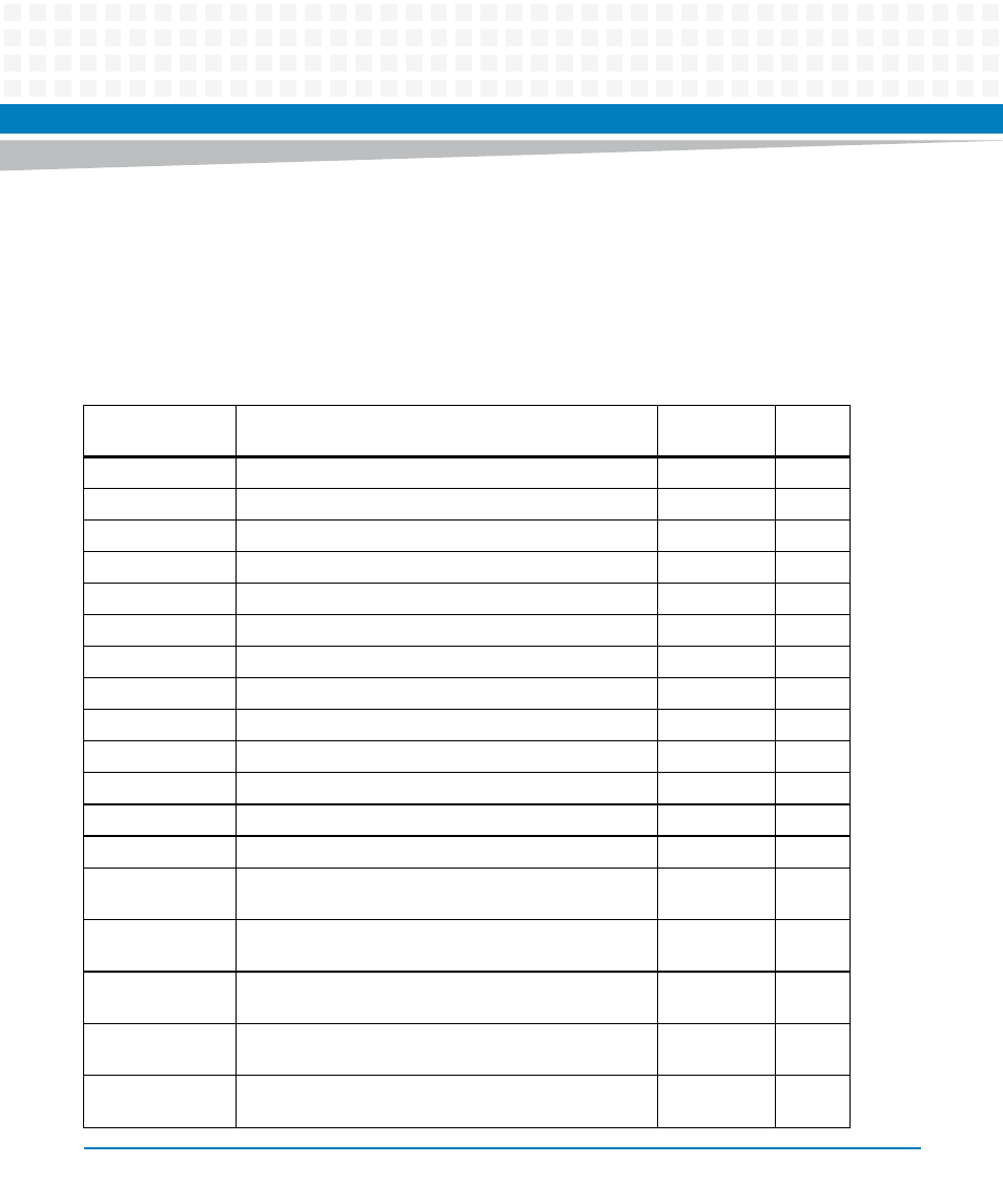
6.1.4
System I/O Memory Map
System resources including System Control and Status registers, external timers, and the
QUART are mapped into a 16MB address range from the MVME3100 via the MPC8540 local bus
controller (LBC). The memory map is defined in the following table, including the LBC bank chip
select used to decode the register:
Table 6-3 System I/O Memory Map
Address
Definition
LBC Bank /
Chip Select
Notes
E200 0000
System Status Register
2
3
E200 0001
System Control Register
2
3
E200 0002
Status Indicator Register
2
3
E200 0003
Flash Control/Status Register
2
3
E200 0004
PCI Bus A Status Register
2
3
E200 0005
PCI Bus B Status Register
2
3
E200 0006
PCI Bus C Status Register
2
3
E200 0007
Interrupt Detect Register
2
3
E200 0008
Presence Detect Register
2
3
E200 0009
PLD Revision
2
3
E200 000C
PLD Date Code (32 bits)
2
3
E200 0010
Test Register 1 (32 bits)
2
3
E200 0014
Test Register 2 (32 bits)
2
3
E200 0018 -
E200 0FFF
Reserved
1
E201 1000 -
E201 1FFF
COM 2 (QUART channel 1)
3
E201 2000 -
E201 2FFF
COM 3 (QUART channel 2)
3
E201 3000 -
E201 3FFF
COM 4 (QUART channel 3)
3
E201 4000 -
E201 4FFF
COM 5 (QUART channel 4)
3