CIRCUTOR CVM-C10 Series User Manual
Page 70
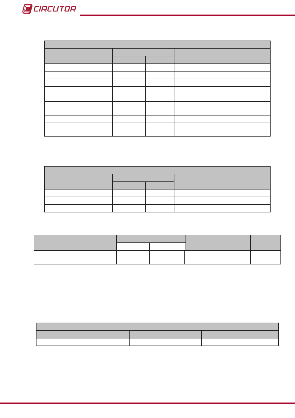
4�10�3�6�11� Programming alarms 1 and 2 (Relays 1 and 2)
Table 33:Modbus memory map: Programming alarms 1 and 2�
Programming alarms 1 and 2
Configuration variable
Address
Valid data margin
Default
value
Relay 1
Relay 2
Maximum value.
2AF8-2AF9 2B02-2B03 depending on the variable
0
Minimum value
2AFA-2AFB 2B04-2B05 depending on the variable
0
Variable code
2AFC
2B06
0
Connection delay
2AFD
2B07
0 - 9999 seconds
0
Hysteresis:
2AFE
2B08
0 - 99 %
0
latch
2AFF
2B09
0 : No
1: Yes
0
Disconnection delay
2B00
2B0A
0 - 9999 seconds
0
Contacts status
2B01
2B0B
0 : Normally open
1: Normally closed
0
4�10�3�6�12� Programming alarms 3 and 4 (Digital outputs T1 and T2)
Table 34:Modbus memory map: Programming alarms 3 and 4�
Programming alarms 3 and 4
Configuration variable
Address
Valid data margin
Default
value
Relay 1
Relay 2
Kilowatts per impulse
2B0C-2B0D 2B16-2B17
0.001 - 999.999 kWh
0
Variable code
2B10
2B1A
0
Pulse width
2B11
2B1B
10 - 500 ms
100 ms
4�10�3�6�13� Digital inputs
Table 35:Modbus memory map: Configuration of digital inputs.
Configuration variable
Address
Valid data margin
Default
value
Input 1
Input 2
Operating mode
(1)
2B66
2B67
0: Tariff
1: Logic state
0
(1)
If Input 1 is configured as a tariff and Input 2 is configured as a logic state (or vice versa) we
will only have 2 tariffs.
We can also read the status of the digital inputs when they are in logic mode:
The
0x04 function is implemented for this variable.
Table 36:Modbus memory map: Status of the digital inputs (Logic state mode)
Status of digital inputs
Variable
Address
Default value
Status of digital inputs
4E20
-
The variable format is shown in
70
CVM-C10
Instruction Manual