Altera DDR Timing Wizard User Manual
Page 46
2–34
Altera Corporation
DDR Timing Wizard User Guide
November 2007
Entering and Editing Inputs to the DTW
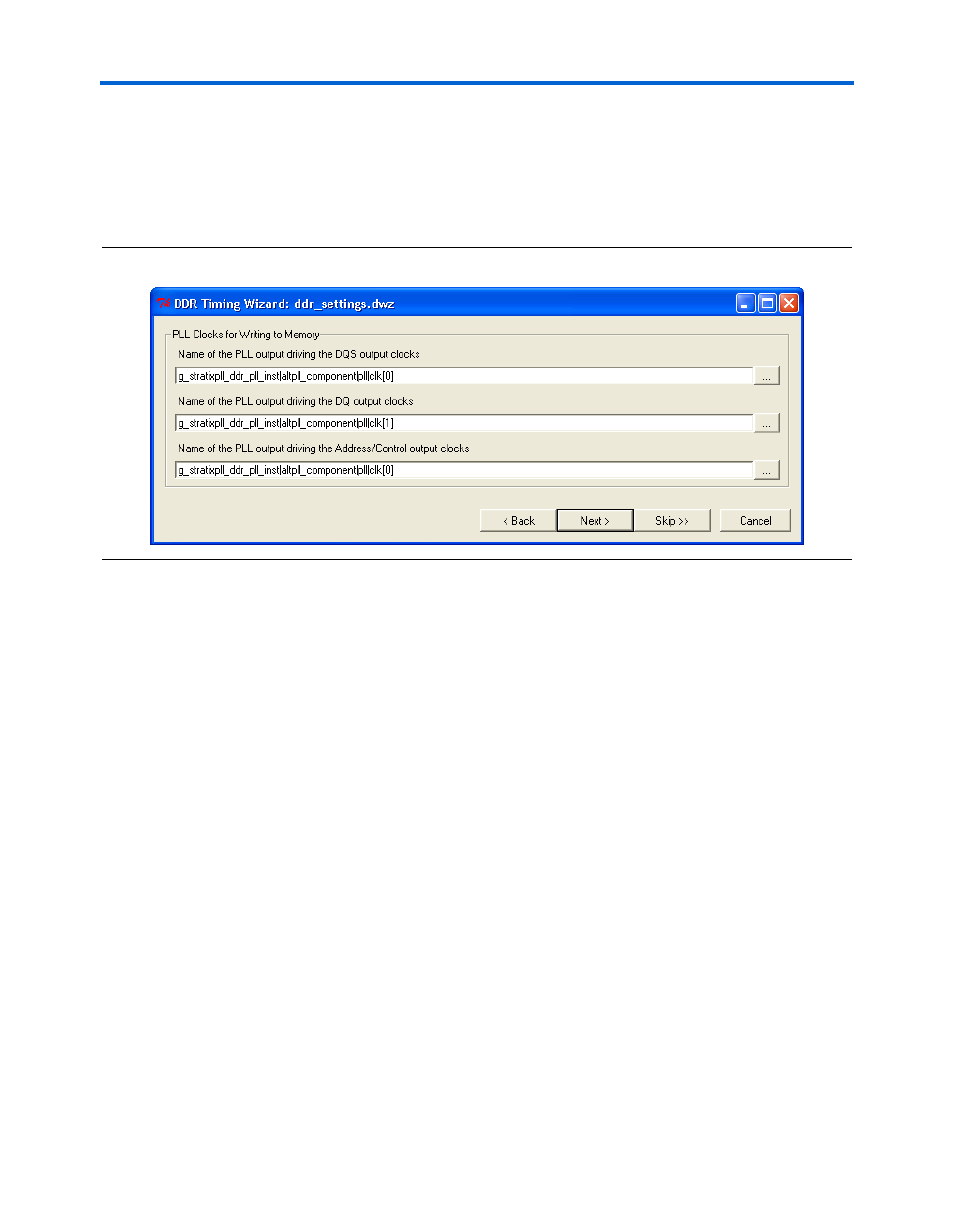
You also must specify which PLL output clock drives the address
and control signals so the DTW can constrain the skew between
those pins and the CK/CK# pins properly. The Altera DDR/DDR2
SDRAM controller uses clk0 and clk1 of the system PLL to
generate DQS and DQ signals, respectively, as shown in
Figure 2–24. Default Clock Selection for the Altera DDR/DDR2 SDRAM Controller
Click Next.
14.
shows the DTW page in which you specify board trace
lengths. This information is required to calculate the
resynchronization and postamble clock phase shifts. The
DDR/DDR2 SDRAM legacy controller MegaWizard has some
default values (as shown in
); however, you should enter
the accurate trace lengths, skew, and board tolerance so that the
DTW can calculate the correct timing constraints for your data
resynchronization and postamble clocks.
1
It is preferred that the trace delay information is extracted
from the board design with a signal integrity tool. If you can
only provide trace lengths and a constant scaling factor (for
example, 166 ps/in), the timing margin analysis will not be
as accurate. The flight time information should be the
nominal delay for each signal, but you also need to
determine a global tolerance for these numbers as well. If an
accurate number cannot be provided for that tolerance, the
DTW defaults to ±5%. Note that if you use a signal integrity
tool to generate the signal delays, you should set the
Output Pin Load
setting to 0 pF since that load capacitance
is factored into the signal delay.