Altera SCFIFO User Manual
Page 25
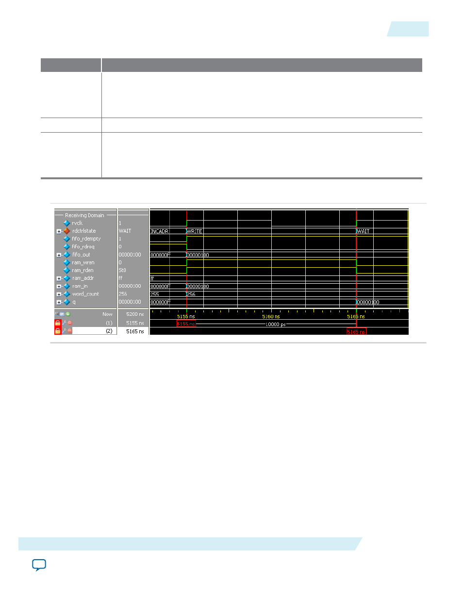
Table 15: Completion of Data Transfer from ROM to DCFIFO Waveform Description
State
Description
WRITE
When the write controller is in the
WRITE
state, and
rom_addr = ff
, the write controller
drives the
fifo_wrreq
signal to high to request for last write operation to DCFIFO. The
data 100 is the last data stored in the ROM to be written into the DCFIFO. In the next
rising clock edge, the write controller transitions to the
DONE
state.
DONE
In the
DONE
state, the write controller drives the
fifo_wrreq
signal to low.
--
The
fifo_wrfull
signal is deasserted because the read controller in the receiving domain
continuously performs the read operation. However, the
fifo_wrfull
signal is only
deasserted sometime after the read request from the receiving domain. This is due to the
latency in the DCFIFO (
rdreq
signal to
wrfull
signal).
Figure 11: Completion of Data Transfer from DCFIFO to RAM
The
fifo_rdempty
signal is asserted to indicate that the DCFIFO is empty. The read controller drives the
fifo_rdreq
signal to low, and enables the write of the last data 100 at
ram_addr =ff
. The
word_count
signal is increased to 256 (in decimal) to indicate that all the 256 words of data from the ROM are success‐
fully transferred to the RAM.
The last data written into the RAM is shown at the
q
output.
Note: To verify the results, compare the
q
outputs with the data in
rom_initdata.hex
file provided in the
design example. Open the file in the Quartus II software and select the word size as 32 bit. The
q
output must display the same data as in the file.
Related Information
Provides all the design files including the testbench. The zip file also includes the .do script
(dcfifo_de_top.do) that automates functional simulation that you can use to run the simulation using the
ModelSim-Altera software
UG-MFNALT_FIFO
2014.12.17
Design Example
25
SCFIFO and DCFIFO IP Cores User Guide
Altera Corporation