Design example, And the read control logic – Altera SCFIFO User Manual
Page 21
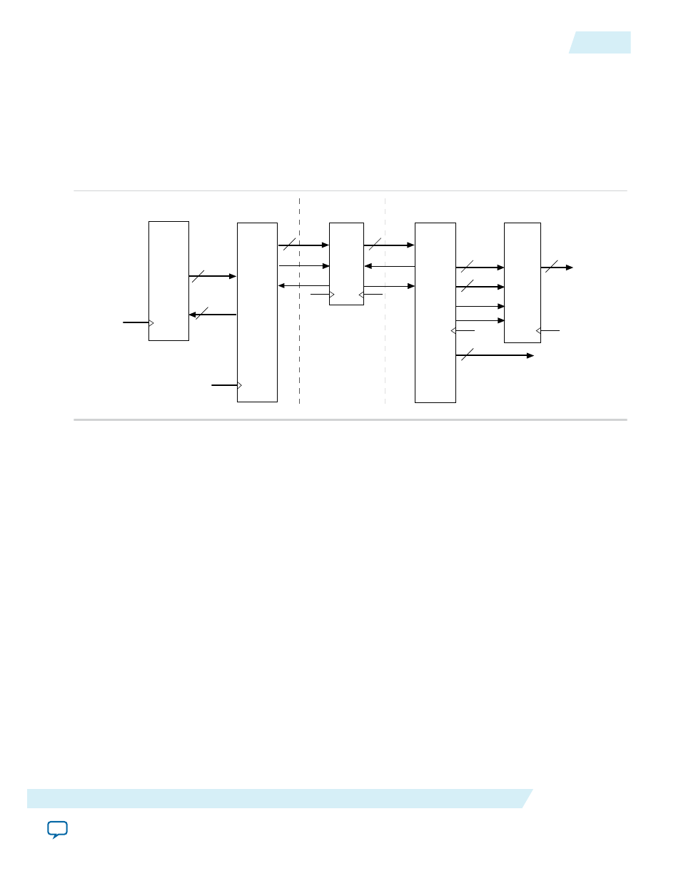
Design Example
In this design example, the data from the ROM is required to be transferred to the RAM. Assuming the
ROM and RAM are driven by non-related clocks, you can use the DCFIFO to transfer the data between
the asynchronous clock domains effectively.
Figure 6: Component Blocks and Signal Interaction
This figure shows the component blocks and their signal interactions.
ROM
256 x 32
trclk
trclk
32
32
fifo_in
fifo_wrreq
fifo_wrfull
trclk
8
rom_out
rom_addr
Write
Control Logic
DCFIFO
8 x 32
Read
Control Logic
RAM
256 x 32
32
fifo_out
32
ram_in
32
q
9
word_count
8
ram_addr
fifo_rdreq
fifo_rdempty
rvclk
rvclk
rvclk
ram_wren
ram_rden
Note: Both the DCFIFO IP cores are only capable of handling asynchronous data transferring issues
(metastable effects). You must have a controller to govern and monitor the data buffering process
between the ROM, DCFIFO, and RAM. This design example provides you the write control logic
(
write_control_logic.v
), and the read control logic (
read_control_logic.v
) which are compiled with the
DCFIFO specifications that control the valid write or read request to or from the DCFIFO.
Note: This design example is validated with its functional behavior, but without timing analysis and gate-
level simulation. The design coding such as the state machine for the write and read controllers
may not be optimized. The intention of this design example is to show the use the IP core, particu‐
larly on its control signal in data buffering application, rather than the design coding and verifica‐
tion processes.
To obtain the DCFIFO settings in this design example, refer to the parameter settings from the design file
(
dcfifo8x32.v
).
The following sections include separate simulation waveforms to describe how the write and read control
logics generate the control signal with respect to the signal received from the DCFIFO.
Note: For better understanding, refer to the signal names in Figure 6 on page 25 when you go through the
descriptions for the simulation waveforms.
UG-MFNALT_FIFO
2014.12.17
Design Example
21
SCFIFO and DCFIFO IP Cores User Guide
Altera Corporation