Constraint settings – Altera SCFIFO User Manual
Page 19

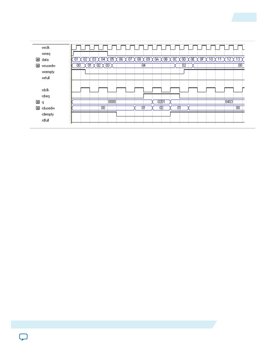
Figure 5: Writing 8-Bit Words and Reading 16-Bit Words
This figure shows an example of a narrow write port (8-bit input) with a wide read port (16-bit output).
In this example, the read port is operating at half the frequency of the write port. Writing four 8-bit words
to the FIFO buffer increases the
wrusedw
flag to four and the
rusedw
flag to two. Two 16-bit read
operations empty the FIFO. The first and second 8-bit word written are equivalent to the LSB and MSB of
the 16-bit output words, respectively. The
rdempty
signal stays asserted until enough words are written on
the narrow write port to fill an entire word on the wide read port.
Constraint Settings
When using the Quartus II TimeQuest timing analyzer with a design that contains a DCFIFO block apply
the following false paths to avoid timing failures in the synchronization registers:
• For paths crossing from the write into the read domain, apply a false path assignment between the
delayed_wrptr_g
and
rs_dgwp
registers:
set_false_path -from [get_registers {*dcfifo*delayed_wrptr_g[*]}] -to [get_registers
{*dcfifo*rs_dgwp*}]
• For paths crossing from the read into the write domain, apply a false path assignment between the
rdptr_g
and
ws_dgrp
registers:
set_false_path -from [get_registers {*dcfifo*rdptr_g[*]}] -to [get_registers
{*dcfifo*ws_dgrp*}]
The false path assignments are automatically added through the HDL-embedded Synopsis design
constraint (SDC) commands when you compile your design. The related message is shown under the
TimeQuest timing analyzer report.
Note: The constraints are internally applied but are not written to the Synopsis Design Constraint File
(.sdc). To view the embedded-false path, type
report_sdc
in the console pane of the TimeQuest
timing analyzer GUI.
If you use the Quartus II Classic timing analyzer, the false paths are applied automatically for the
DCFIFO.
Note: If the DCFIFO is implemented in logic elements (LEs), you can ignore the cross-domain timing
violations from the data path of the DFFE array (that makes up the memory block) to the
q
output
UG-MFNALT_FIFO
2014.12.17
Constraint Settings
19
SCFIFO and DCFIFO IP Cores User Guide
Altera Corporation
