Vga interface lvds interface, Table 3-14, Vga interface pin signals (j3) – ADLINK LittleBoard 735 User Manual
Page 42: Table 3-15, Lvds interface pin signals (j26)
Chapter 3
Hardware
36
Reference Manual
LittleBoard 735
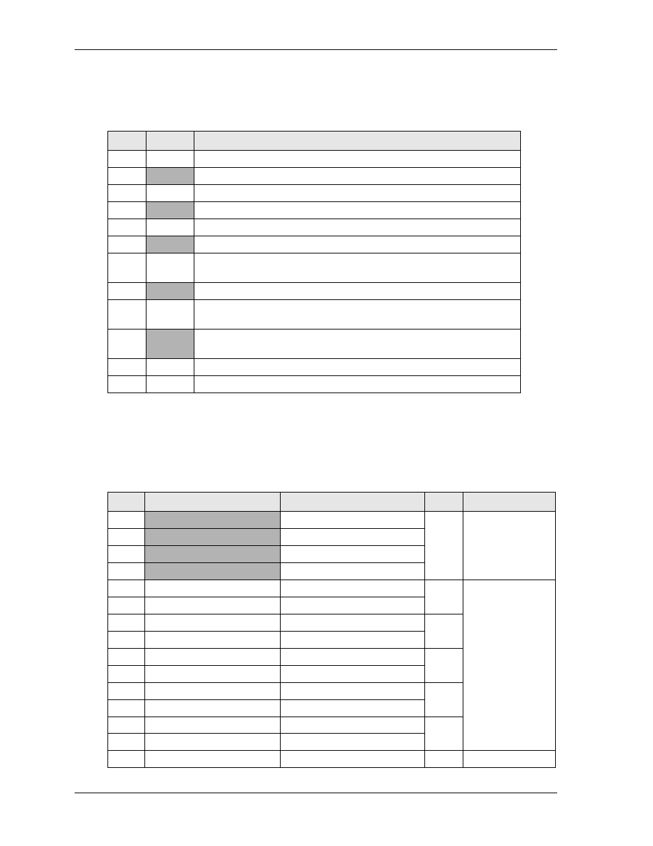
VGA Interface
describes the pin signals of the VGA interface, which uses 12 pins, 2 rows, odd/even sequence
(1, 2) with 0.079" (2mm) pitch.
Note: The shaded table cells denote power or ground.
LVDS Interface
describes the pin signals of the LVDS interface, which provides a 30-pin header with 2 rows,
odd/even sequence (1, 2), and 0.079" (2mm) pitch.
Table 3-14. VGA Interface Pin Signals (J3)
Pin #
Signal
Description
1
RED
Red – This is the Red analog output signal to the CRT.
2
GND
Ground (Red Return)
3
GREEN
Green – This is the Green analog output signal to the CRT.
4
GND
Ground (Green Return)
5
BLUE
Blue – This is the Blue analog output signal to the CRT.
6
GND
Ground (Blue Return)
7
HSYNC
Horizontal Sync – This signal is used for the digital horizontal sync output
to the CRT.
8
GND
Ground
9
VSYNC
Vertical Sync – This signal is used for the digital vertical sync output to
the CRT.
10
PWR
Power – Provided through fuse (F1) to +5 volts +/- 5%. F1 is next to J3
connector on board.
11
SDA
DDC (Display Data Channel) Data
12
SCL
DDC (Display Data Channel) Clock
Table 3-15. LVDS Interface Pin Signals (J26)
Pin #
Signal
Description
Line
Channel
1
+12V
+12 volt input
NA
NA
2
+VCC (+3.3V/+5V)
JP1 determines voltage on pin
3
GND
Ground
4
GND
Ground
5
LBCLK_P
Clock Positive Output
Clock
Channel 2
6
LBCLK_N
Clock Negative Output
7
Not Supported
N/A
N/S
8
Not Supported
N/A
9
LBDATA2_P
Data Positive Output
2
10
LBDATA2_N
Data Negative Output
11
LBDATA1_P
Data Positive Output
1
12
LBDATA1_N
Data Negative Output
13
LBDATA0_P
Data Positive Output
0
14
LBDATA0_N
Data Negative Output
15
LVDS_BKLT_CTL
Control Panel Backlight
NA
NA