Figure 2-5, Pin sequence identification – ADLINK LittleBoard 735 User Manual
Page 19
Chapter 2
Product Overview
LittleBoard 735
Reference Manual
13
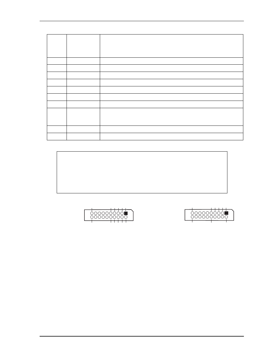
Figure 2-5. Pin Sequence Identification
J38
Latch (on back
of the board;
see
Latch for the PCI Express Mini Card connector
J39
USB 4 & 5
10-pin, 0.079" (2mm) header for USB4 and USB5 ports
J40
GPIO
10-pin, 0.079" (2mm) header for General Purpose IO signals
J41
DNP
Do not populate
J42
DNP
Do not populate
J43
DNP
Do not populate
J44
USB 0 & 1
10-pin, 0.079" (2mm) header for USB0 and USB1 ports
J45
SMBus
5-pin, 0.049" (1.25mm) header for external device connection
J46
Power On
Button and
Reset Switch
5-pin header for power-on button and reset switch
J47
LED - GLAN1
5-pin, 0.049" (1.25mm) header for Gigabit Ethernet1 external LED
J48
LED - GLAN2
5-pin, 0.049" (1.25mm) header for Gigabit Ethernet2 external LED
NOTE
The pinout tables in Chapter 3 of this manual identify pin sequence using the
following methods: A 20-pin header with two rows of pins, using odd/even
numbering, where pin 2 is directly across from pin 1, is noted as 20-pin, 2 rows,
odd/even (1, 2). Alternately, a 20-pin connector using consecutive numbering,
where pin 11 is directly across from pin 1, is noted in this way: 20-pin, 2 rows,
consecutive (1, 11). The second number in the parenthesis is always directly
across from pin 1. See
.
Table 2-2. Header and Connector Descriptions (Continued)
20-pin, two rows,
Consecutive, (1, 11)
Or
1
2
3
4
5
6
7
8
9
10
20
19
1
2
4
15
11
20
10
5 3
20-pin, two rows,
Odd/Even, (1, 2)
LB735_ConNum