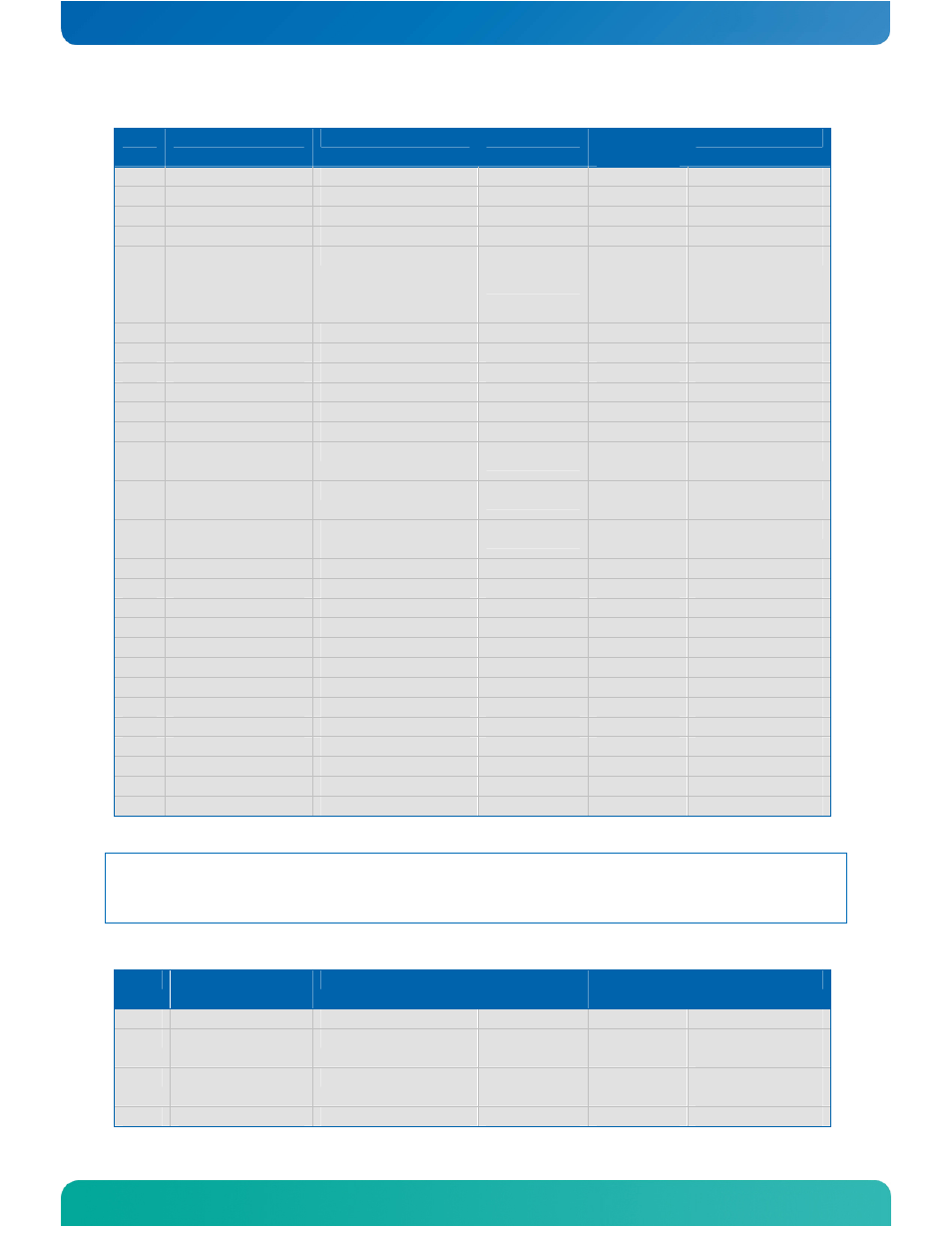
Table 7: connector x1b - row c – Kontron COMe-cPV2(v1.4) User Manual
Page 29
Kontron microETXexpress-PV User’s Guide
25
Pin
Signal
Description
Type
Terminati
on
Comment
B84
VCC_5V_SBY
+5V Standby
PWR
-
-
B85
VCC_5V_SBY
+5V Standby
PWR
-
-
B86
VCC_5V_SBY
+5V Standby
PWR
-
-
B87
VCC_5V_SBY
+5V Standby
PWR
-
-
B88
BIOS_DIS1#
BIOS Disable
I – 3.3 SUS
PU 3.3V
SUS of
51.1K
ohms
-
B89
VGA_RED
Analog video
O - Analog
-
-
B90
GND (Fixed)
Power Ground
PWR
-
-
B91
VGA_GRN
Analog video
O - Analog
-
-
B92
VGA_BLU
Analog video
O - Analog
-
-
B93
VGA_HSYNC
Horizontal Sync
O - 3.3
-
-
B94
VGA_VSYNC
Vertical Sync
O - 3.3
-
-
B95
VGA_I2C_CK
DDC Clock
I/0 - 3.3
PU 3.3V
of 4.75K
-
B96
VGA_I2C_DAT
DDC Data
I/O – 3.3
PU 3.3V
of 4.75K
-
B97
SPI_CS#
Carrier board SPI
chip select
O – 3.3 SUS
-
B98
RSVD
Reserved
-
-
-
B99
RSVD
Reserved
-
-
-
B100
GND (Fixed)
Power Ground
PWR
-
-
B101
RSVD
Reserved
-
-
-
B102
RSVD
Reserved
-
-
-
B103
RSVD
Reserved
-
-
-
B104
VCC_12V
12V VCC
PWR
-
-
B105
VCC_12V
12V VCC
PWR
-
-
B106
VCC_12V
12V VCC
PWR
-
-
B107
VCC_12V
12V VCC
PWR
-
-
B108
VCC_12V
12V VCC
PWR
-
-
B109
VCC_12V
12V VCC
PWR
-
-
B110
GND (Fixed)
Power Ground
PWR
NOTE: The termination resistors in this table are already mounted on the
ETXexpress® board. Refer to the PICMG COM Express® Design Guide for
information about additional termination resistors.
Table 7: Connector X1B - Row C
Pin
Signal
Description
Type
Terminati
on
Comment
C1
GND (Fixed)
Power Ground
PWR
-
-
C2
IDE_D7
IDE Data Bus 7
I/O – 3.3
-
5V tolerant
input
C3
IDE_D6
IDE Data Bus 6
I/O – 3.3
-
5V tolerant
input
C4
IDE_D3
IDE Data Bus 3
I/O – 3.3
-
5V tolerant