1) on a standard vm162/vm172 board, these signals, 2) on a standard vm162/vm172 board, these signals, 3) on pa13, a 24 mhz clock signal is routed via ju – Kontron VM162 User Manual
Page 49: 4) these signals are routed both to the base board
VM162/VM172
Chapter 2 Functional Description
Juli 23, 1997
Page 2- 27
© PEP Modular Computers
Notes:
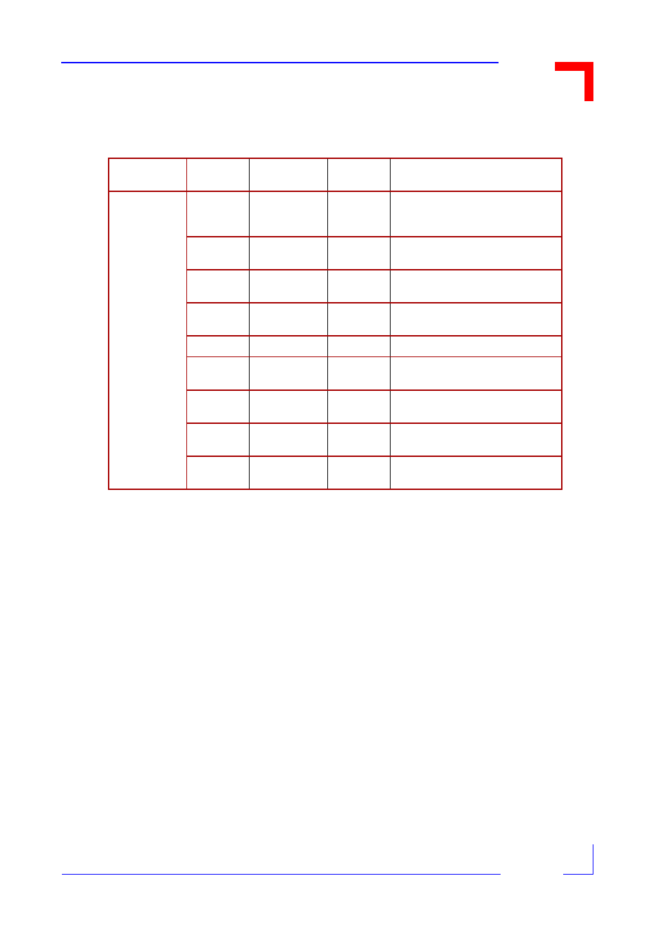
Reserved Pins
1) On a standard VM162/VM172 board, these signals are already used for UART ports at BU7 and
BU8.
2) On a standard VM162/VM172 board, these signals are used for SPI to which the EEPROM is
already connected. PB0 is chip select of the EEPROM.
3) On PA13, a 24 MHz clock signal is routed via jumper J11. This signal is always needed for PEP
standard software (serial drivers).
Dual Functioning Signal Pins
4) These signals are routed both to the base board SI Interface connector (ST5C) and the CXC con-
nector and can only be used by one or the other and not both at the same time.
Due to this, a conflict exists if the SCC4 port is to be used with the SI232 piggyback and CXC boards
(such as CXM-SIO3), as both boards access this port. The SCC4 port can, therefore, not be used at
the
same time by SI piggybacks and CXC boards.
CXC
Function
Pin Nr.
68302 HW
Compatible
68(EN)360
Port
Comment
user defined
a5
No
PB0
Used on board SPI SEL for EEPROM.
Cannot be used on CXC
See note 2
a6
No
PB1
SPI Clk: can be used if an ‘SPI SEL’
other than PB0 is used
a8
No
PB2
SPI TxD: can be used if an ‘SPI SEL’
other than PB0 is used
a9
No
PB3
SPI RxD: can be used if an ‘SPI SEL’
other than PB0 is used
a10
No
PB8
See 68360 User Manual
b11
No
PB10
Used on board SMC2 (Transmit)
See note 1
c1
No
PB6
Used on board SMC1 (Transmit)
See note 1
c4
No
PB11
Used on board SMC2 (Receive)
See note 1
c10
No
PB7
Used on board SMC1 (Receive)
See note 1