Rockwell Automation 1771-N SERIES High Resolution Analog Module User Manual User Manual
Page 86
Specifications
A–6
Publication 1771ĆUM127B-EN-P - December 2002
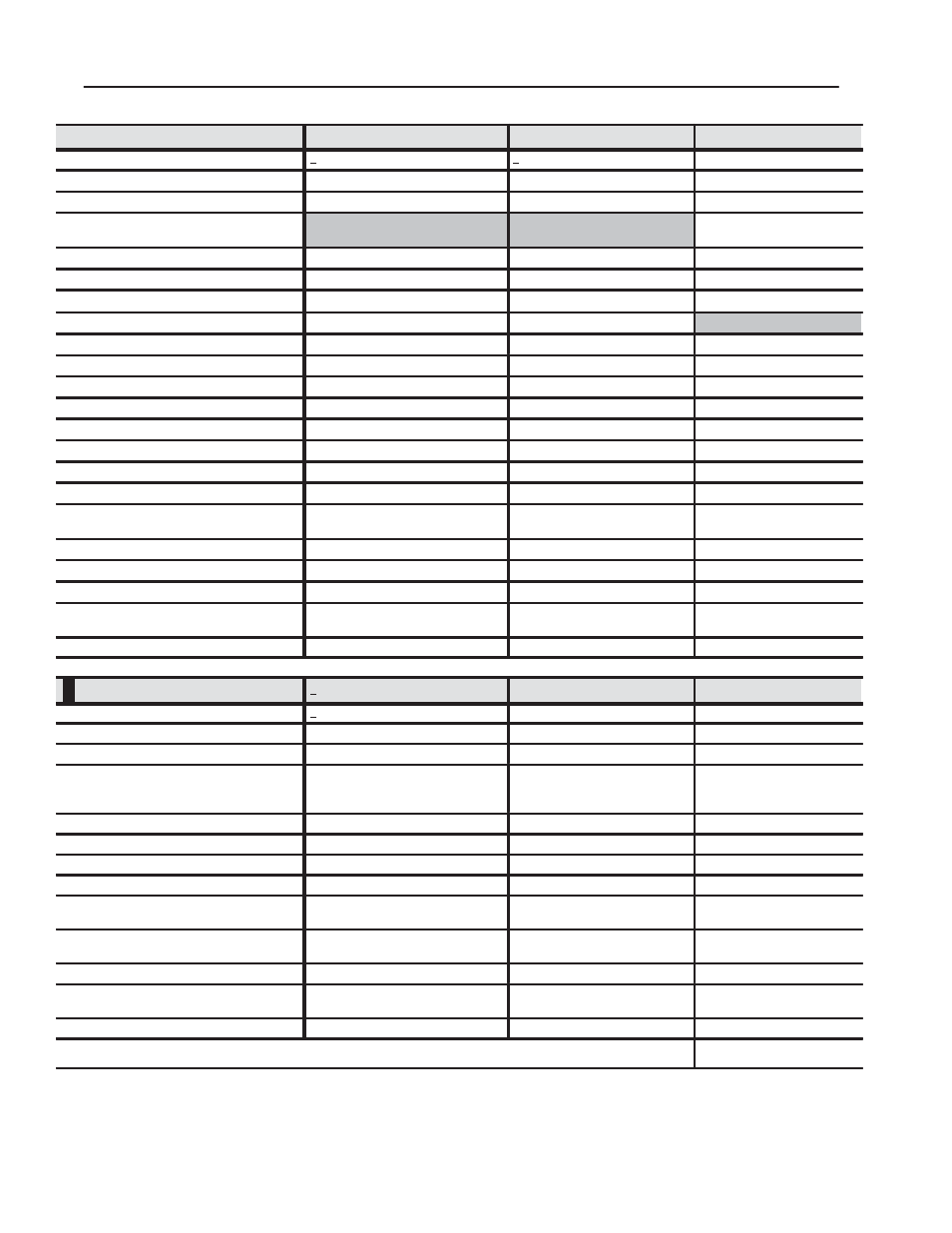
±5V Inputs
±10V Inputs
4Ć20mA Sourcing Input
Input Range
+5.5V (±22mA with resistor)
+10.5V (±42mA with resistor)
0.1Ć21.0mA
Input Resolution
168µV/bit (0.7µA/bit) 15 bits with sign bit
330µV/bit 15 bits with sign bit
330nA/bit 16 bits unipolar
Input Impedance
> 10 MΩ
> 10 MΩ
300Ω (maximum)
Loop Power Voltage Source
20 to 30V dc (0 to 20mA range)
current limited to < 29mA
Input Overvoltage Protection
140V ac rms continuous
140V ac rms continuous
24V dc continuous
Open Input Detection
upscale
upscale
downscale
Time to Detect Open Input
5s (maximum)
9s (maximum)
5s (maximum)
Open Input Detection Leakage Current
< 1.0µA (maximum)
< 1.0µA (maximum)
Normal Mode Rejection 50/60Hz
50dB / 60dB (minimum)
50dB / 60dB (minimum)
50dB / 60dB (minimum)
Common Mode Rejection (60Hz)
150dB (typical)
150dB (typical)
150dB (typical)
Offset Drift
±20µV/
o
C (±85nA/°C with resistor)
±30 µV/
o
C
±200nA/°C
Gain Drift
±35 ppm/
o
C (±55ppm/°C with resistor)
±35 ppm/
o
C
±95 ppm/
o
C
Input Bandwidth
9Hz
9Hz
9Hz
Update Time (per module)
25ms (maximum)
25ms (maximum)
25ms (maximum)
SettlingTime to within 0.1% of Full Scale
125ms (maximum)
125ms (maximum)
125ms (maximum)
NonĆlinearity
0.02% of full range (maximum)
0.02% of full range (maximum)
0.02% of full range (maximum)
Accuracy with Calibration (includingtypical
nonĆlinearity, gain,and offset)
worst case
0.01% of full range @ 25
o
C
0.05% of full range @ 25
o
C
0.01% of full range @ 25
o
C
0.05% of full range @ 25
o
C
0.025% of full range @ 25
o
C
0.05% of full range @ 25
o
C
Calibration Values
0.0000V / 5.0000V
0.0000V / 10.0000V
1.000mA / 21.000mA
Underrange Threshold
0.8V dc (3.2mA)
-10.4V dc
3.2mA
Overrange Threshold
5.2V dc (20.8mA)
+10.4V dc
21.0mA
Rate Alarm Value
minimum (0.04% FSR)
maximum (50% FSR)
1.6mV (6.4µA) per second
2.0V (8.0mA) per second
8mV per second
10V per second
6.4µA per second
8mA per second
ScalingPoints → Default ScalingValues
1
1.0/5.0V
→
1000/5000
-10 / +10V → -10000/+10000
4.0/20.0mA → 4000/20000
+10V Outputs
4-20mA (0-25mA) Outputs
0-50mA Outputs
Output Range
+10.4V into an open circuit
0Ć25.0mA
0Ć50.0mA
Output Resolution
1.32mV/bit 13 bits with sign bit
3.2µA/bit 13 bits unipolar
6.4µA/bit 13 bits unipolar
Output Impedance
1.0Ω maximum
> 1 MΩ
> 1 MΩ
Output Drive Capability
1KΩ or larger (10mA maximum)
20.0mA maximum into 0Ć1kΩ
25.0mA maximum into 0Ć700Ω
20.0mA maximum into 0Ć1kΩ
25.0mA maximum into 0Ć700Ω
50.0mA maximum into 0Ć300Ω
2
Output Overvoltage Protection
140V ac rms continuous
140V ac rms continuous
140V ac rms continuous
Offset Drift
±400 µV/°C
±1.0µA/
o
C
±1.0µA/
o
C
Gain Drift
±50 ppm/
o
C
±50 ppm/
o
C
±50 ppm/
o
C
Update Time (per module)
25ms maximum
25ms maximum
25ms maximum
D/A Converter Ċ SettlingTime to within
10% of Full Scale into a Resistive Load
5ms
500µs
500µs
Accuracy with Calibration (Includingtypical
NonĆlinearity, Gain, and Offset)
worst case
0.01% of full range @ 25
o
C
0.08% of full range @ 25
o
C
0.01% of full range @ 25
o
C
0.08% of full range @ 25
o
C
0.01% of full range @ 25
o
C
0.08% of full range @ 25
o
C
Calibration Values
0.0/10.0V dc
0.5mA / 22.0 mA
1.0mA / 50.0 mA
RampingValue
minimum (1% FSR)
maximum (200% FSR)
0.2V per second
40.0V per second
0.16mA per second
32.0mA per second
0.40mA per second
80.0mA per second
ScalingPoints → Default ScalingValues
1
-10 / +10V
→ -10,000/+10,000
4.0 / 20.0mA → 4,000/20,000
10.0 / 50.0mA → 1,000/5,000
1
Values shown are applicable when usingtwo's complement data format.
2
See deratingcurves for various temperature, current and load conditions.