Pin descriptions - software (hardware) mode, Cs42l51 – Cirrus Logic CS42L51 User Manual
Page 7
DS679F1
7
CS42L51
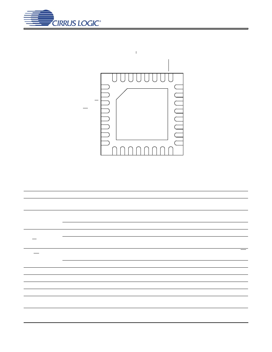
1. PIN DESCRIPTIONS - SOFTWARE (HARDWARE) MODE
Pin Name
#
Pin Description
LRCK
1
Left Right Clock (Input/Output) - Determines which channel, Left or Right, is currently active on the
serial audio data line.
SDA/CDIN
(MCLKDIV2)
2
Serial Control Data (Input/Output) - SDA is a data I/O in I²C Mode. CDIN is the input data line for the
control port interface in SPI Mode.
MCLK Divide by 2 (Input) - Hardware Mode: Divides the MCLK by 2 prior to all internal circuitry.
SCL/CCLK
(I²S/LJ)
3
Serial Control Port Clock (Input) - Serial clock for the serial control port.
Interface Format Selection (Input) - Hardware Mode: Selects between I²S & Left-Justified interface for-
mats for the ADC & DAC.
AD0/CS
(DEM)
4
Address Bit 0 (I²C) / Control Port Chip Select (SPI) (Input) - AD0 is a chip address pin in I²C Mode; CS
is the chip-select signal for SPI format.
De-Emphasis (Input) - Hardware Mode: Enables/disables the de-emphasis filter.
VA_HP
5
Analog Power For Headphone (Input) - Positive power for the internal analog headphone section.
FLYP
6
Charge Pump Cap Positive Node (Input) - Positive node for the external charge pump capacitor.
GND_HP
7
Analog Ground (Input) - Ground reference for the internal headphone/charge pump section.
FLYN
8
Charge Pump Cap Negative Node (Input) - Negative node for the external charge pump capacitor.
VSS_HP
9
Negative Voltage From Charge Pump (Output) - Negative voltage rail for the internal analog head-
phone section.
10
9
8
7
6
5
4
3
2
1
11
12
13
14
15
16
17
18
19
20
21
22
23
24
25
26
27
28
29
30
31
32
CS42L51
VD
DGND
SDO
U
T (M/S
)
MCLK
SDIN
SC
L
K
V
SS_HP
AO
UT
B
AO
UTA
VA
AG
ND
DAC_F
ILT+
ADC_F
ILT+
VQ
SDA/CDIN (MCLKDIV2)
SCL/CCLK (I²S/LJ)
ADO/CS (DEM)
FLYP
VL
RE
SET
GND_HP
FLYN
AFILTA
AIN1A
AIN1B
AIN2A
AIN2B/BIAS
MICIN1/AIN3A
MICIN2/BIAS/AIN3B
AFILTB
VA_HP
LRCK