3 multiplexing configuration, Multiplexing configuration, Table 3-5 – AMD Geode SC3200 User Manual
Page 45: Two-signal/group multiplexing, Section 3.3 "multiplexing configuration
AMD Geode™ SC3200 Processor Data Book
45
32581C
3.3
Multiplexing Configuration
The tables that follow list multiplexing options and their
configurations. Certain multiplexing options may be chosen
per signal; others are available only for a group of signals.
Where ever a GPIO pin is multiplexed with another func-
tion, there is an optional pull-up resistor on this pin; after
system reset, the pull-up is present. This pull-up resistor
can be disabled by writing Core Logic registers. The config-
uration is without regard to the selected ball function. The
above applies to all pins multiplexed with GPIO, except
GPIO12, GPIO13, and GPIO16.
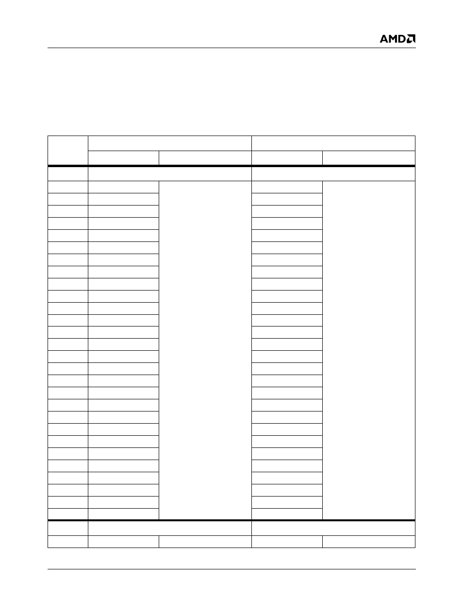
Table 3-5. Two-Signal/Group Multiplexing
Ball No.
Default
Alternate
Signal
Configuration
Signal
Configuration
IDE
TFT, PCI, GPIO, System
AD3
IDE_ADDR0
PMR[24] = 0
TFTD3
PMR[24] = 1
AE1
IDE_ADDR1
TFTD2
U2
IDE_ADDR2
TFTD4
AC3
IDE_DATA0
TFTD6
AC1
IDE_DATA1
TFTD16
AC2
IDE_DATA2
TFTD14
AB4
IDE_DATA3
TFTD12
AB1
IDE_DATA4
FP_VDD_ON
AA4
IDE_DATA5
CLK27M
AA3
IDE_DATA6
IRQ9
AA2
IDE_DATA7
INTD#
Y3
IDE_DATA8
GPIO40
Y2
IDE_DATA9
DDC_SDA
Y1
IDE_DATA10
DDC_SCL
W4
IDE_DATA11
GPIO41
W3
IDE_DATA12
TFTD13
V3
IDE_DATA13
TFTD15
V2
IDE_DATA14
TFTD17
V1
IDE_DATA15
TFTD7
Y4
IDE_IOR0#
TFTD10
AD1
IDE_IORDY0
TFTD11
AC4
IDE_DREQ0
TFTD8
AD2
IDE_IOW0#
TFTD9
AF2
IDE_CS0#
TFTD5
P2
IDE_CS1#
TFTDE
AD4
IDE_DACK0#
TFTD0
AA1
IDE_RST#
TFTDCK
AF1
IRQ14
TFTD1
Sub-ISA
GPIO
D11
TRDE#
PMR[12] = 0
GPIO0
PMR[12] = 1