Table 5-50, Bank 3 register map, Table 5-51 – AMD Geode SC3200 User Manual
Page 135: Bank 4 register map, Table 5-52, Bank 5 register map
AMD Geode™ SC3200 Processor Data Book
135
SuperI/O Module
32581C
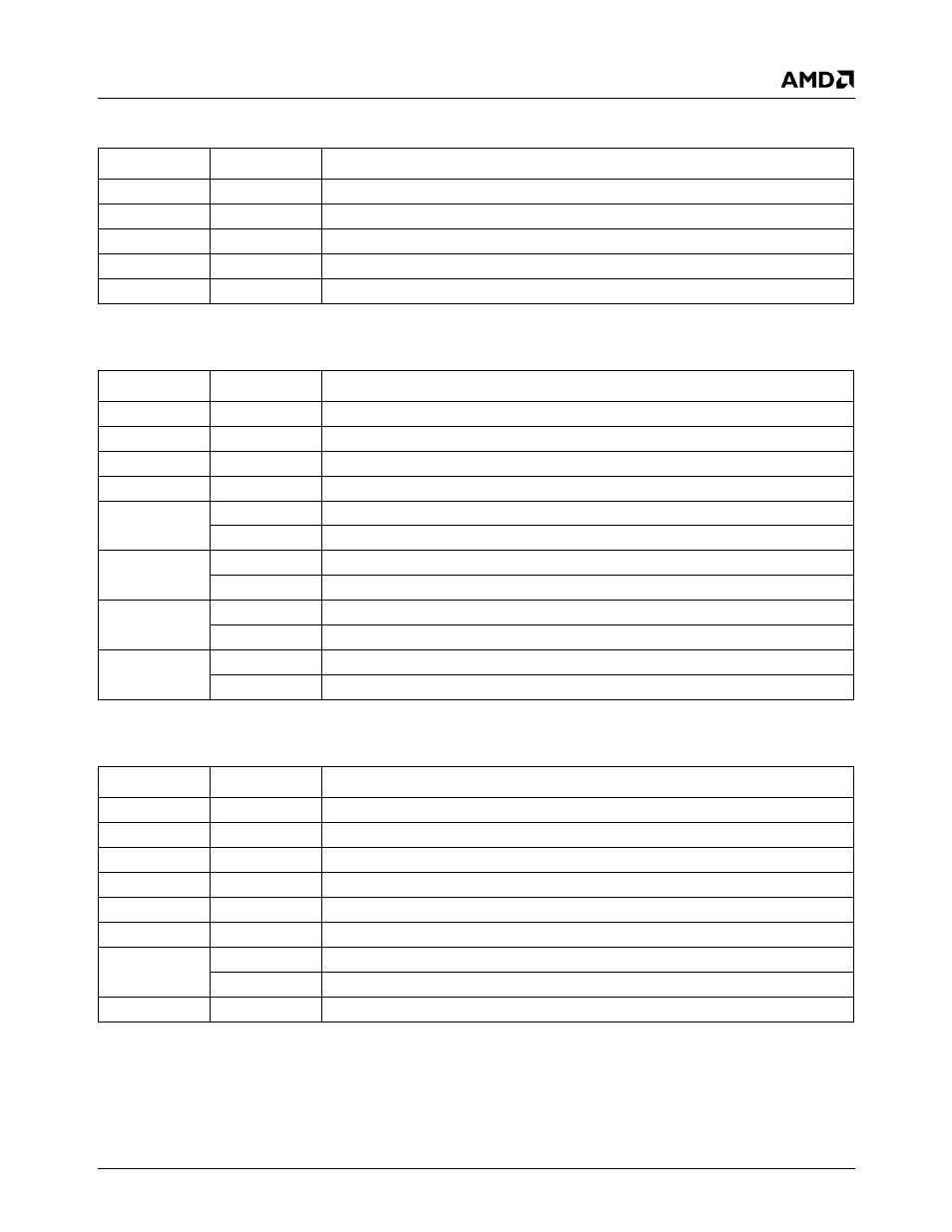
Table 5-50. Bank 3 Register Map
Offset
Type
Name
00h
RO
MID. Module and Revision Identification
01h
RO
SH_LCR. Link Control Shadow
02h
RO
SH_FCR. FIFO Control Shadow
03h
R/W
BSR. Bank Select
04h-07h
---
RSVD. Reserved
Table 5-51. Bank 4 Register Map
Offset
Type
Name
00h
RO
TMR(L). TImer (Low Byte)
01h
RO
TMR(H). Timer (High Byte)
02h
R/W
IRCR1. IR Control 1
03h
R/W
BSR. Bank Select
04h
R/W
TFRL(L). Transmission Frame Length (Low Byte)
RO
TFRCC(L). Transmission Current Count (Low Byte)
05h
R/W
TFRL(H). Transmission Frame Length (High Byte)
RO
TFRCC(H). Transmission Current Count (High Byte)
06h
R/W
RFRML(L). Reception Frame Maximum Length (Low Byte)
RO
RFRCC(L). Reception Frame Current Count (Low Byte)
07h
R/W
RFRML(H). Reception Frame Maximum Length (High Byte)
RO
RFRCC(H). Reception Frame Current Count (High Byte)
Table 5-52. Bank 5 Register Map
Offset
Type
Name
00h
R/W
SPR3. Scratchpad 2
01h
R/W
SPR3. Scratchpad 3
02h
R/W
RSVD. Reserved
03h
R/W
BSR. Bank Select
04h
R/W
IRCR2. IR Control 2
05h RO
FRM_ST. Frame Status
06h
RO
RFRL(L). Received Frame Length (Low Byte)
RO
LSTFRC. Lost Frame Count
07h
RO
RFRL(H). Received Frame Length (High Byte)