Table 9-12, Memory controller timing parameters – AMD Geode SC3200 User Manual
Page 364
364
AMD Geode™ SC3200 Processor Data Book
Electrical Specifications
32581C
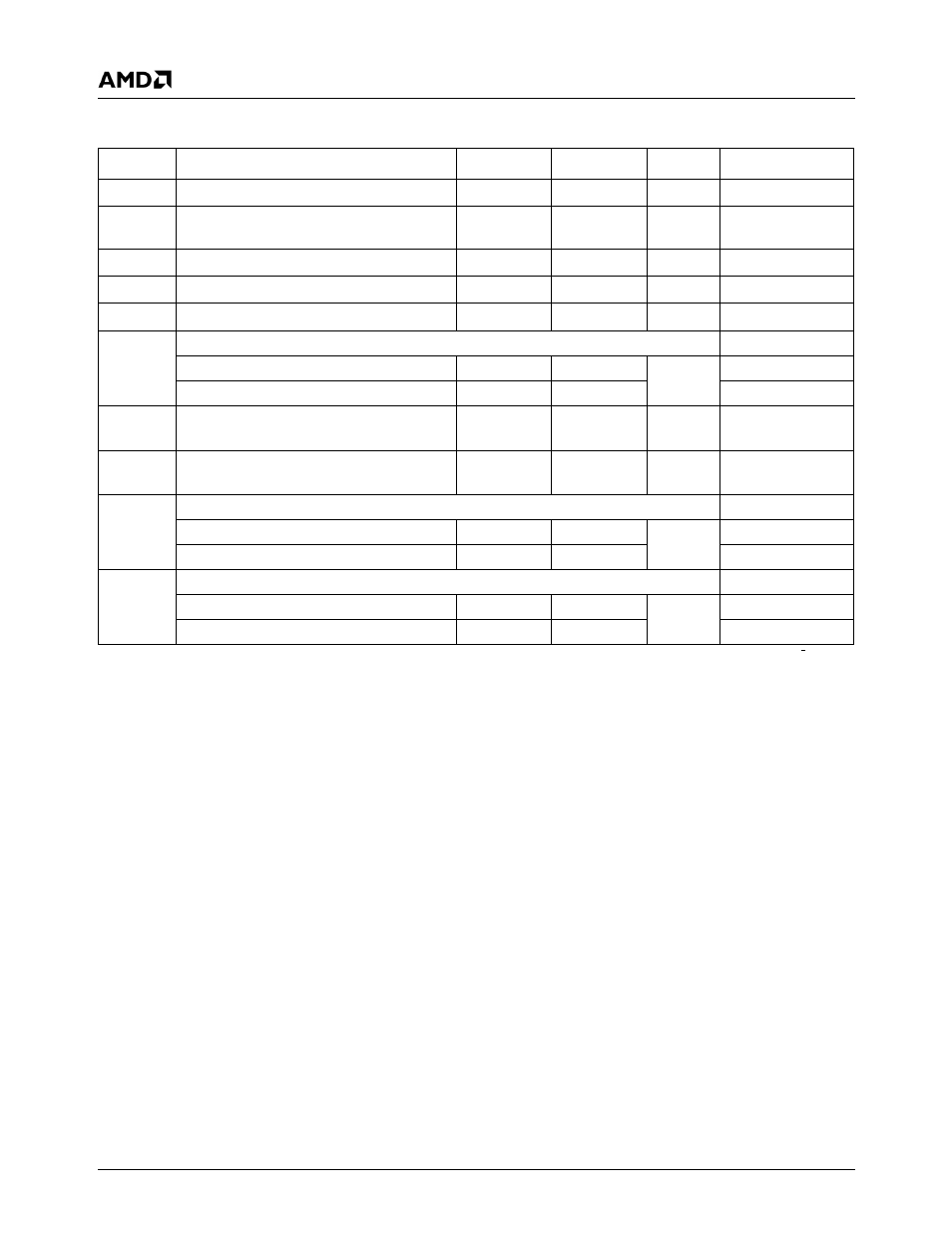
Table 9-12. Memory Controller Timing Parameters
Symbol
Parameter
Min
Max
Unit
Comments
t
1
Control output valid from SDCLK[3:0]
-3.0 + (x
*
y)
0.1 + (x
*
y)
ns
Note 1, Note 2
t
2
MA[12:0], BA[1.0] output valid from
SDCLK[3:0]
-3.2 + (x
*
y)
0.1 + (x
*
y)
ns
Note 2
t
3
MD[63.0] output valid from SDCLK[3:0]
-2.2 + (x
*
y)
0.7 + (x
*
y)
ns
Note 2
t
4
MD[63.0] read data in setup to SDCLK_IN
1.3
ns
t
5
MD[63:0] read data hold to SDCLK_IN
2.0
ns
t
6
SDCLK[3:0], SDCLK_OUT cycle time
233 MHz
10
14
ns
266 MHz
8.3
13.5
t
7
SDCLK[3:0], SDCLK_OUT fall/rise time
between (V
OLD
-V
OHD
)
2
ns
t
9
SDCLK_IN fall/rise time between
(V
ILD
-V
IHD
)
2
ns
t
10
SDCLK[3:0], SDCLK_OUT high time
233 MHz
4.0
ns
266 MHz
3.0
t
11
SDCLK[3:0], SDCLK_OUT low time
233 MHz
4.0
ns
266 MHz
2.5
Note 1. Control output includes all the following signals: RASA#, CASA#, WEA#, CKEA, DQM[7:0], and CS[1:0]#.
Load = 50 pF, V
CORE
= 1.8V@ 233/266 MHz, V
IO
= 3.3V, @25
o
C.
Note 2. Use the Min/Max equations [value+(x * y)] to calculate the actual output value.
x is the shift value which is applied to the SHFTSDCLK field, and y is 0.45 the core clock period.
Note that the SHFTSDCLK field = GX_BASE+Memory Offset 8404h[5:3]. Refer to the AMD Geode™ GX1 Proces-
sor Data Book for more information.
For example, for a 266 MHz SC3200 running a 88.7 MHz SDRAM clock, with a shift value of 3:
t1 Min = -3 + (3 * (3.76 * 0.45)) = 2.08 ns
t1 Max = 0.1 + (3 * (3.76 * 0.45)) = 5.18 ns