3 tft interface, Figure 9-7, Tft timing diagram – AMD Geode SC3200 User Manual
Page 367: Table 9-14, Tft timing parameters
AMD Geode™ SC3200 Processor Data Book
367
Electrical Specifications
32581C
9.3.3
TFT Interface
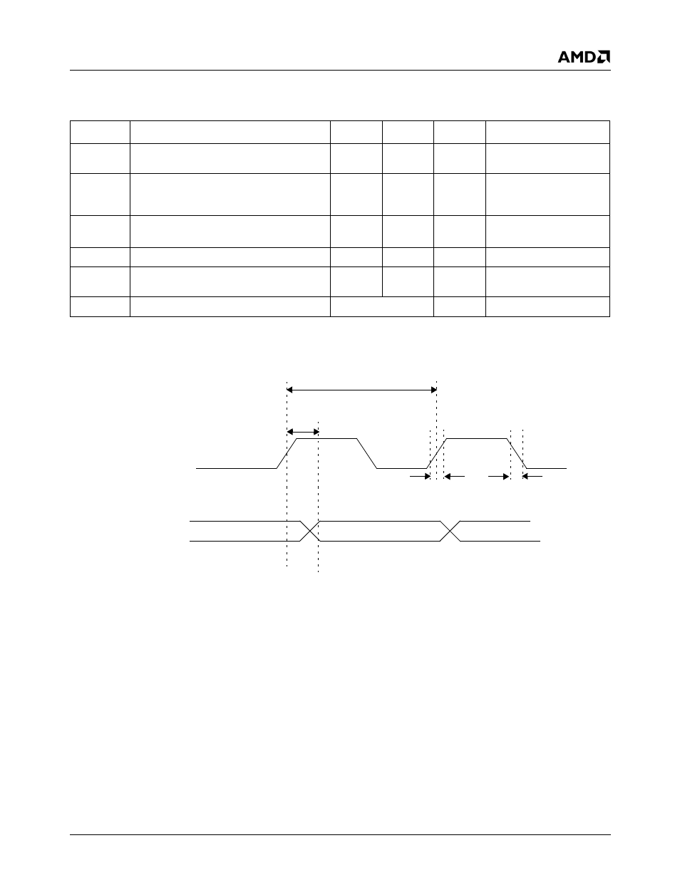
Figure 9-7. TFT Timing Diagram
Table 9-14. TFT Timing Parameters
Symbol
Parameter
Min
Max
Unit
Comments
t
OV
TFTD[17:0], TFTDE valid time after
TFTDCK rising edge (multiplexed on IDE)
0
8
ns
t
OV
TFTD[17:0], TFTDE valid time after
TFTDCK rising edge (multiplexed on
Parallel Port)
0
4
ns
t
CLK_RF
TFTDCK rise/fall time
between 0.8V and
2.0V
3
ns
Note 1
t
CLK_P
TFTDCK period time (multiplexed on IDE)
25
ns
t
CLK_P
TFTDCK period time (multiplexed on
Parallel Port)
12.5
ns
t
CLK_D
TFTDCK duty cycle
40/60
%
Note 1. Guaranteed by characterization
t
OV
t
CLK_RF
t
CLK_P
TFTDCK
TFTD[17:0]
TFTDE
See also other documents in the category AMD Hardware:
- Radeon 4850 (18 pages)
- Phenom AM2r2 (6 pages)
- GA-K8N51GMF-9 (80 pages)
- Socket AM2+ Quad Core Processor SB750 (63 pages)
- Turion 64 X2 (2 pages)
- GA-M61PM-S2 (80 pages)
- Socket AM2+ Quad Core AMD Processor 790GX (53 pages)
- 7ZMMC (36 pages)
- Geode SC1200 (443 pages)
- CS5535 (36 pages)
- Geode LX800 (46 pages)
- ATI RADEON HD 2600 (62 pages)
- LE-363 (45 pages)
- SimNow Simulator 4.4.4 (269 pages)
- GA-MA69VM-S2 (88 pages)
- KM780V (21 pages)
- SBX-5363 (55 pages)
- AM79C971 (1 page)
- K3780E-S (43 pages)
- GEODE LE-366 (45 pages)
- 7ZX-1 (46 pages)
- Geode SC2200 (429 pages)
- Phenom II (6 pages)
- ATI Radeon x1700 FSC (22 pages)
- Turion 64 (3 pages)
- 1207 (62 pages)
- CrossFire 550X (16 pages)
- Athlon 27488 (104 pages)
- Geode LX [email protected] (680 pages)
- GA-M61SME-S2 (80 pages)
- N2PA-LITE (45 pages)
- GA-K8NSC-939 (80 pages)
- GEODE NX800LX (27 pages)
- Am79C930 (161 pages)
- LV-651 (50 pages)
- Athlon 6 (19 pages)
- SEMPRON 10 (102 pages)
- GA-K8N ULTRA-9 (80 pages)
- Geode LX CS5536 (8 pages)
- MINI-ITX LV-651 (50 pages)
- GA-K8N51GMF-RH (88 pages)
- ATI RADEON HD 2400 (64 pages)
- GA-M55S-S3 (88 pages)
- GA-M51GM-S2G (88 pages)