4 tft interface, Figure 7-13, Tft power sequence – AMD Geode SC3200 User Manual
Page 325

AMD Geode™ SC3200 Processor Data Book
325
Video Processor Module
32581C
7.2.4
TFT Interface
The TFT interface can be programmed to one of two sets of
balls: IDE balls or Parallel Port balls. PMR[23] of the Gen-
eral Configuration registers program where the TFT inter-
face exists (see Table 4-2 on page 70).
Note:
If the TFT interface is on the IDE balls, the maxi-
mum FPCLK supported is 40 MHz. If the TFT inter-
face is on the Parallel Port balls the maximum
FPCLK supported is 80 MHz.
Support for a TFT panel requires power sequencing and an
18-bit (6-bit RGB), digital output. The relevant digital output
signals are available from the SC3200.
TFT output signals are:
• TFTD[5:0] for blue signals
• TFTD[11:6] for green signals
• TFTD[17:12] for red signals
• HSYNC and VSYNC - sync signals
• TFTDCK - data clock signal.
• TFTDE - data enable signal.
• FP_VDD_ON - power control signal
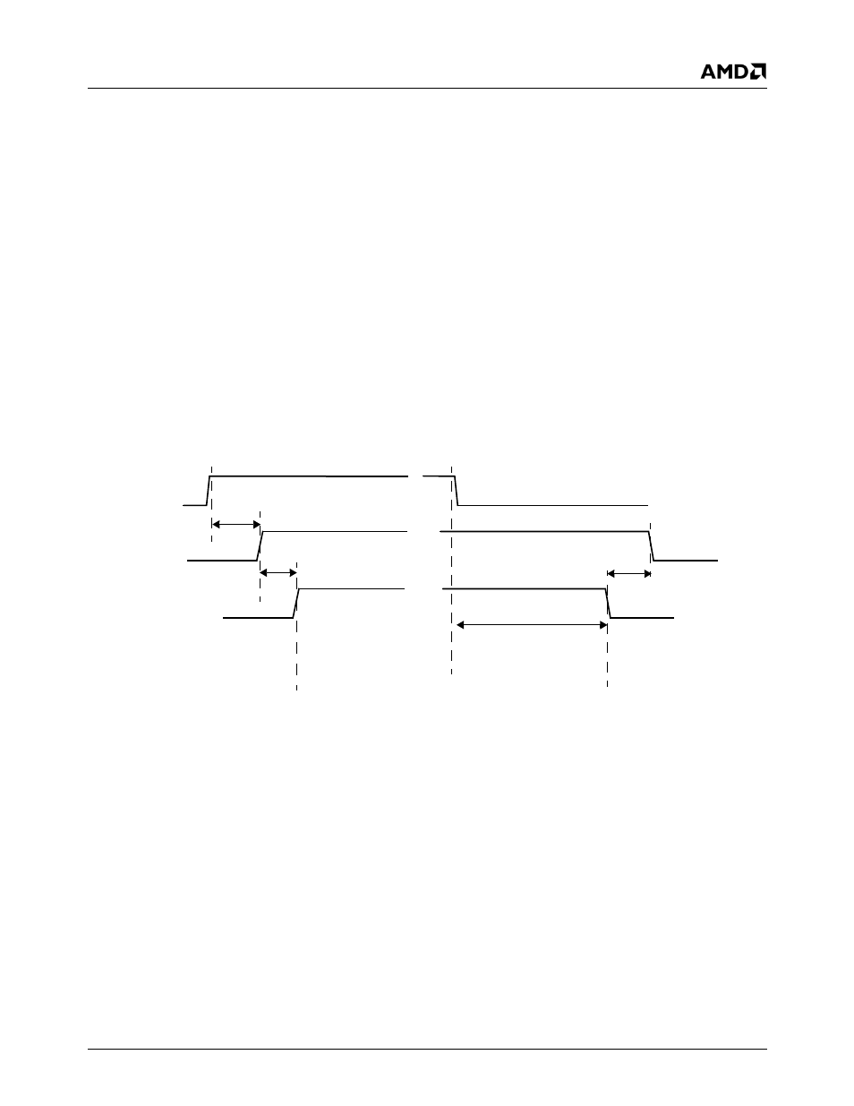
Power Sequence
Power sequence is used to control assertion of
FP_VDD_ON and TFTD signals.
All bits related to power sequence configuration are located
in the Display Configuration register (F4BAR0+Memory
Offset 04h).
After enabling TFT_EN (bit 0), and FP_PWR_EN (bit 6),
the state machine waits until the next VSYNC to switch on
the FP_VDD_ON signal. The state machine then asserts
the TFTD[17:0] signals after the delay programmed via
PWR_SEQ_DLY (bits [19:17]) When FP_PWR_EN (bit 6)
is set to 0, the reverse sequence happens for powering
down the TFT.
Figure 7-13. TFT Power Sequence
FP_VDD_ON
FP_PWR_EN
TFTD[17:0],
HSYNC, VSYNC,
TFTDE, TFTDCK
T
1
T
1
T
0
+T
1
T
0
T
0
is time to next VSYNC
T
1
is a programmable multiple of frame time
bit
