3 digital input/output (dio) connector, Figure 4-3: audio connector location, Table 4-4: audio connector pinouts – IEI Integration PCIE-Q350 v1.30 User Manual
Page 69: See figure 4-3, See table 4-4
PCIE-Q350 PICMG 1.3 CPU Card
Page 49
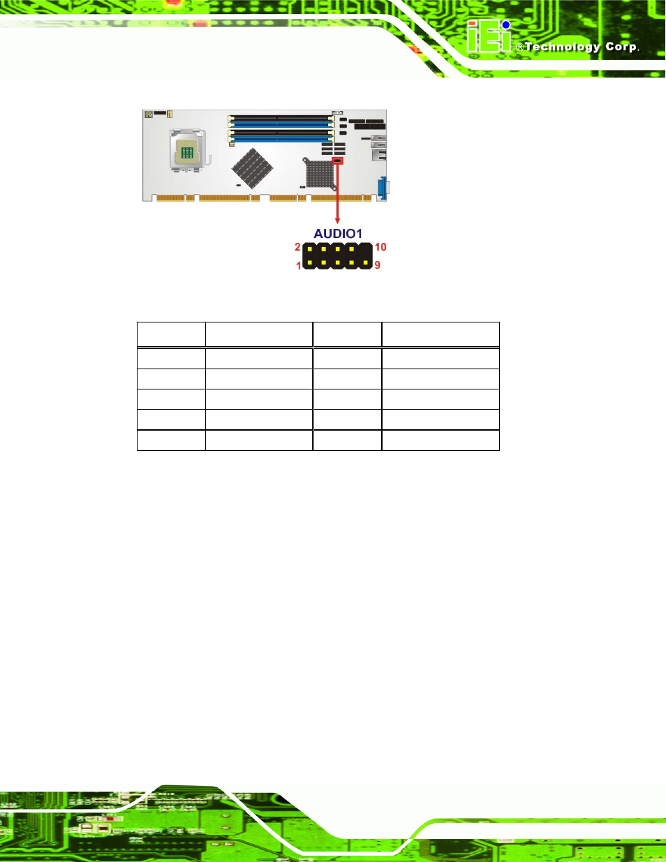
Figure 4-3: Audio Connector Location
PIN NO.
DESCRIPTION
PIN NO.
DESCRIPTION
1 SYNC
2 BITCLK
3 SDOUT
4 PCBEEP
5 SDIN
6 RST#
7 VCC
8 GND
9 +12V
10
N/C
Table 4-4: Audio Connector Pinouts
4.2.3 Digital Input/Output (DIO) Connector
CN Label:
DIO1
CN Type:
18-pin header (2x9)
CN Location:
CN Pinouts:
The digital input/output connector is managed through a Super I/O chip. The DIO
connector pins are user programmable. To see details on how to program the DIO chip,
please refer to Appendix B.
See also other documents in the category IEI Integration Hardware:
- SPCIE-5100DX (180 pages)
- SPCIE-C2060 v1.01 (200 pages)
- SPCIE-C2060 v2.12 (212 pages)
- SPCIE-C2160 (204 pages)
- SPCIE-C2260-i2 (217 pages)
- ROCKY-3786 v4.0 (175 pages)
- ROCKY-3786 v4.10 (147 pages)
- PCIE-Q350 v1.00 (272 pages)
- PCIE-Q350 v1.12 (250 pages)
- PCIE-Q350 v1.20 (250 pages)
- PCIE-Q57A (159 pages)
- PCIE-G41A2 (151 pages)
- PCIE-Q670 v1.03 (206 pages)
- PCIE-Q670 v2.00 (205 pages)
- PCIE-H610 (181 pages)
- PCIE-Q870-i2 (217 pages)
- IOWA-LX-600 (159 pages)
- PCISA-945GSE v1.01 (207 pages)
- PCISA-945GSE v1.10 (190 pages)
- PCISA-9652 v1.00 (232 pages)
- PCISA-9652 v1.01 (232 pages)
- PCISA-PV-D4251_N4551_D5251 (145 pages)
- PICOe-945GSE (197 pages)
- PICOe-GM45A (198 pages)
- PICOe-PV-D4251_N4551_D5251 v1.00 (154 pages)
- PICOe-PV-D4251_N4551_D5251 v1.10 (154 pages)
- PICOe-PV-D4251_N4551_D5251 v1.11 (155 pages)
- PICOe-B650 (156 pages)
- PICOe-HM650 (174 pages)
- HYPER-KBN (139 pages)
- SPXE-14S (3 pages)
- SPXE-9S v1.00 (5 pages)
- SPXE-9S v1.1 (6 pages)
- SPE-9S v1.00 (4 pages)
- SPE-9S v1.1 (5 pages)
- SPE-6S (3 pages)
- SPE-4S (4 pages)
- PE-6SD3 (4 pages)
- PE-6SD2 v4.0 (4 pages)
- PE-6SD2 v2.10 (3 pages)
- PE-6SD (3 pages)
- PE-6S3 v1.0 (2 pages)
- PE-6S3 v4.0 (4 pages)
- PE-6S2 (4 pages)