Figure 3-5 – Atec Tektronix-1502 User Manual
Page 32

TM 9-4935-601-14-3&P
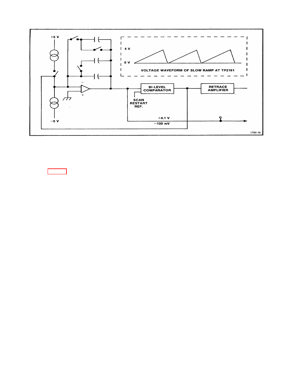
Figure 3-5. Functional Block Diagram of Slow Ramp Generator.
Integrator. An inverting amplifier circuit with an FET input is used as an integrator. Integrator capacitor
C2356 is connected between the collector of Q2345 and the inverting input (gate of Q2246A). A minus current
applied to the inverting input through R2353 results in a linear rising voltage on the output (see the waveform
shown in Fig. 3-5). This output voltage will continue to rise until it reaches the internal comparison level of 4.1
volts. The bi-level comparator output then switches to a higher output level to close FET switch Q2257. It also
changes its comparison level to -.1 V. This allows a positive current to be applied to the input of the integrator.
The positive current is several times larger than the negative current and causes the output voltage of the
integrator to decrease linearly. After a short period of time, the integrator output voltage approaches this
comparison voltage of -0.1 V and causes the positive current into the integrator to be turned off. At this time
the comparator level is switched back to the 4.1 V level and the cycle starts over.
The rise and fall time of the slow ramp can be varied by changing the integrating capacitance values. In
the normal 40 Hz scan frequency, a value of 0.0013
µ
F is used. When NOISE FILTER switch S2254 is
activated, the scan frequency is reduced by approximately 7 times by paralleling a capacitance value of 0.01
µ
F to the original 0.0013
µ
F. For recording (X-Y or chart) purposes, a value of 1
µ
F is used. (Q2248 acts as a
FET switch and is controlled by the Record Logic.)
Bi-Level Comparator. During the positive going sequence of the Slow Ramp Generator, Q2261 is
saturated and Q2262 is off. The emitter voltage of Q2261 and Q2262 is 4.1 volts. This voltage is controlled by
a resistor divider, R2267 and R2158. The collector (output of the comparator) of Q2262 is at a -5 V level
because the transistor is not conducting. The anode of CR2161 has to rise to 4.1 volts in order to turn off
Q2261.
When Q2261 turns off, its collector level will decrease, which causes Q2262 to be turned on and saturated.
The emitter voltage output switches to -0.1 volt. 02261 remains off until the anode voltage of CR2161 goes to -
0.1 volt, which restarts the cycle.
The comparator can be forced into the scan cycle when the Recorder Logic turns on CR2262.
Retrace Signal Amplifier. The retrace signal amplifier uses an input FET (Q2258) to drive amplifier
Q2259. The output voltage is +5 V during retrace and -5 V during the scan cycle. The output is used for Chart
Recorder Logic and Record Logic.
Current Sources. The positive and negative currents for the retrace sweep are generated by applying +5
V and -5 V to the high value resistors R2251 and R2353 respectively.
REV A FEB 1980
3-7
