C/spi interface – Rainbow Electronics MAX1386 User Manual
Page 9

MAX1385/MAX1386
Dual RF LDMOS Bias Controllers
with I
2
C/SPI Interface
_______________________________________________________________________________________
9
Note 1: Guaranteed by design.
Note 2: Total unadjusted errors are for the entire gain drive channel including the 8- and 10-bit DACs and the gate driver. They are
all measured at the GATE1 and GATE2 outputs. Offset removal refers to presetting the drain current after a room tempera-
ture calibration by the user. This effectively removes the channel offset.
Note 3: During power-on reset, the output safe switch is closed. The output safe switch opens once both AV
DD
and DV
DD
supply
voltages are established.
Note 4: Integral nonlinearity is the deviation of the analog value at any code from its theoretical value after the gain and offset errors
have been removed.
Note 5: Offset nulled.
Note 6: Absolute range for analog inputs is from 0 to AV
DD
.
Note 7: The MAX1385/MAX1386 and external sensor are at the same temperature. External sensor measurement error is tested with
a diode-connected 2N3904.
Note 8: The drive current ratio is defined as the large drive current divided by the small drive current in a temperature measure-
ment. See the
Temperature Measurements section for further details.
Note 9: Guaranteed monotonicity. Accuracy might be degraded at lower V
REFDAC
.
Note 10: Supply current limits are valid only when digital inputs are at DV
DD
or DGND. Timing specifications are only guaranteed
when inputs are driven rail-to-rail.
Note 11: Shutdown supply currents are typically 0.1µA. Maximum specification is limited by automated test equipment.
Note 12: All timing specifications referred to V
IH
or V
IL
levels.
Note 13: A master device must provide a hold time of at least 300ns for the SDA signal (referred to V
IL
of SCL) to bridge the unde-
fined region of SCL’s falling edge.
Note 14: C
b
= total capacitance of one bus line in pF; t
R
and t
F
are measured between 0.3 x DV
DD
and 0.7 x DV
DD
.
Note 15: For a device operating in an I
2
C-compatible system.
Note 16: Input filters on the SDA and SCL inputs suppress noise spikes less than 50ns.
Note 17: A device must provide a data hold time to bridge the undefined part between V
IH
and V
IL
of the falling edge of the SCL signal.
An input circuit with a threshold as low as possible for the falling edge of the SCL signal minimizes this hold time.
Note 18: Cb = total capacitance of one bus line in pF. For bus loads between 100pF and 400pF, the timing parameters should be
linearly interpolated.
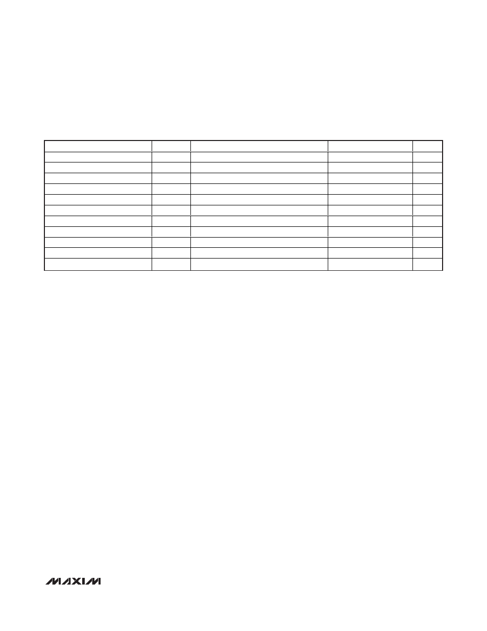
SPI TIMING CHARACTERISTICS (Note 12, See Figure 3)
(GATEV
DD
= +5.5V for the MAX1385, GATEV
DD
= +11V for the MAX1386, AV
DD
= +5V, DV
DD
= 2.7V to 5.25V, external V
REFADC
=
+2.5V, external V
REFDAC
= +2.5V, C
REF
= 0.1µF, T
A
= -40°C to +85°C, unless otherwise noted.)
PARAMETER
SYMBOL
CONDITIONS
MIN
TYP
MAX
UNITS
SCL Clock Period
t
CP
62.5
ns
SCL High Time
t
CH
25
ns
SCL Low Time
t
CL
25
ns
DIN Setup Time
t
DS
10
ns
DIN Hold Time
t
DH
0
ns
SCL Fall to DOUT Transition
t
DO
C
LOAD
= 30pF
20
ns
CSB Fall to DOUT Enable
t
DV
C
LOAD
= 30pF
40
ns
CSB Rise to DOUT Disable
t
TR
C
LOAD
= 30pF (Note 12)
100
ns
CSB Rise or Fall to SCL Rise
t
CSS
25
ns
CSB Pulse-Width High
t
CSW
100
ns
Last Clock Rise to
CSB Rise
t
CSH
50
ns
