C/spi interface, Table 23. fifo (read), Table 24. rdfine1 and rdfine2 (read) – Rainbow Electronics MAX1386 User Manual
Page 39
MAX1385/MAX1386
Dual RF LDMOS Bias Controllers
with I
2
C/SPI Interface
______________________________________________________________________________________
39
16 bits of data from a MAX1385/MAX1386 register (see
Figure 11):
1) After generating a START condition (S or Sr),
address the MAX1385/MAX1386 by sending the
appropriate slave address byte and its correspond-
ing R/
W bit set to a 0 (see the
Slave Address Byte
section). The MAX1385/MAX1386 then answer with
an ACK bit (see the
Acknowledge Bits
section).
2) Send the appropriate read command byte (see the
Command Byte
section). The MAX1385/MAX1386
answer with an ACK bit.
3) After generating a repeated START condition (Sr),
address the MAX1385/MAX1386 once more by
sending the appropriate slave address byte and its
R/
W bit set to 1. The MAX1385/MAX1386 answer
with an ACK bit.
4) The MAX1385/MAX1386 transmit the most signifi-
cant 8-bit data byte of the 16-bit data word with the
MSB first. Afterwards, the master needs to send an
ACK bit.
5) The MAX1385/MAX1386 transmit the least signifi-
cant 8-bit byte of the 16-bit word with the MSB first.
6) The master issues a NACK bit and then generates a
repeated START or STOP condition (Sr or P).
Continue to poll the current register or read multiple
words (e.g., empty FIFO of several conversion results)
by omitting step 6 and keep issuing ACK bits after each
data byte. Use the following 3-byte sequence to read
16 bits of data from the last accessed MAX1385/
MAX1386 register:
1) After generating a START condition (S or Sr),
address the MAX1385/MAX1386 by sending the
appropriate 7-bit slave address byte and its corre-
sponding R/
W bit set to 1 (see the
Slave Address
Byte
section). The MAX1385/MAX1386 then answer
with an ACK bit (see the
Acknowledge Bits
section).
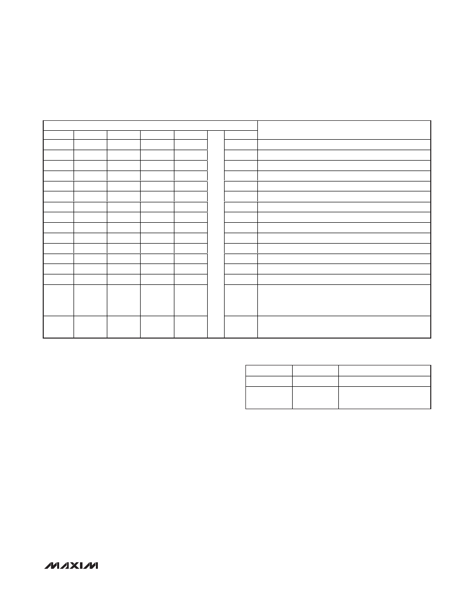
DATA BITS
D15
D14
D13
D12
D11
D0
CONVERSION ORIGIN
0
0
0
0
MSB
LSB
Internal temperature sensor
0
0
0
1
MSB
LSB
Channel 1 external temperature
0
0
1
0
MSB
LSB
Channel 1 drain current (PGAOUT1)
0
0
1
1
MSB
LSB
ADCIN1
0
1
0
0
MSB
LSB
Channel 2 external temperature
0
1
0
1
MSB
LSB
Channel 2 drain current (PGAOUT2)
0
1
1
0
MSB
LSB
ADCIN2
0
1
1
1
—
—
Reserved
1
0
0
0
—
—
Reserved
1
0
0
1
—
—
Reserved
1
0
1
0
—
—
Reserved
1
0
1
1
—
—
Reserved
1
1
0
0
—
—
Reserved
1
1
0
1
—
—
Reserved
1
1
1
0
MSB
LSB
Conversion may be corrupted. This occurs only when
arriving data causes the FIFO to overflow at the same time
data is being read out.
1
1
1
1
MSB
BITS D11–D0 CONTAIN THE CONVERSION RESULT
LSB
Empty FIFO. The current value of the Flag register is
provided in place of the FIFO data.
Table 23. FIFO (Read)
DATA BITS
POR
FUNCTION
D15–D10
X
Don’t care.
D9–D0
00 0000 0000
10-bit fine DAC input code.
D9 is the MSB.
Table 24. RDFINE1 and RDFINE2 (Read)