C/spi interface, Pin description (continued) – Rainbow Electronics MAX1386 User Manual
Page 16
MAX1385/MAX1386
Dual RF LDMOS Bias Controllers
with I
2
C/SPI Interface
16
______________________________________________________________________________________
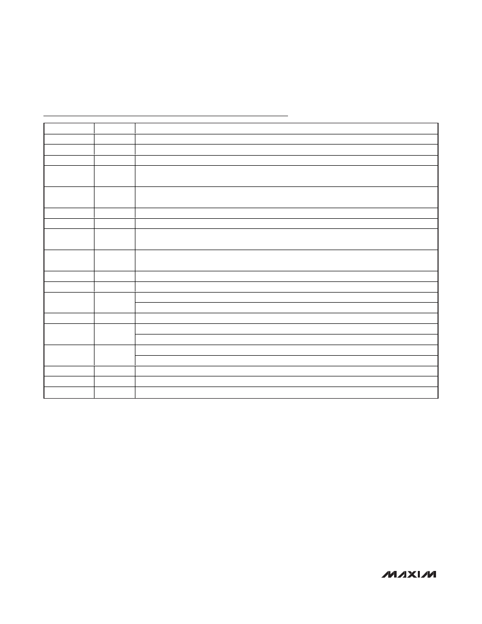
Pin Description (continued)
PIN
NAME
FUNCTION
23
GATEGND
Gate-Drive Amplifier Ground
24
GATEV
DD
Gate-Drive Amplifier Supply Input
26
OPSAFE2
Operating Safe Channel 2 Input. Drive OPSAFE2 high to clamp GATE2 to AGND.
27
CS2+
Current-Sense Positive Input 2. CS2+ is the external sense resistor connection to the LDMOS 2
supply.
29
CS2-
Current-Sense Negative Input 2. CS2- is the external sense resistor connection to the LDMOS 2
drain.
30
GATE2
Channel 2 Gate-Drive Amplifier Output
31
GATE1
Channel 1 Gate-Drive Amplifier Output
32
CS1-
Current-Sense Negative Input 1. CS1- is the external sense resistor connection to the LDMOS 1
drain.
33
CS1+
Current-Sense Positive Input 1. CS1+ is the external sense resistor connection to the LDMOS 1
supply.
34
OPSAFE1
Operating Safe Channel 1 Input. Drive OPSAFE1 high to clamp GATE1 to AGND.
40
PGAOUT1
Programmable-Gain Amplifier Output 1
I
2
C-Compatible Address 2. See the Digital Serial Interface section.
41
A2/N.C.
No Connection. Leave unconnected in SPI mode.
43
SCL
Digital Serial Clock Input
I
2
C-Compatible Serial Data Input/Output
44
SDA/DIN
SPI-Compatible Serial Data Input
I
2
C-Compatible Address 1. See the Digital Serial Interface section.
45
A1/DOUT
SPI-Compatible Serial Data Output
47
BUSY
Device Busy Output. See the BUSY Output section
48
DV
DD
Digital Supply Input
—
EP
Exposed Pad. Connect to AGND. Internally connected to analog ground.