C/spi interface, Acknowledge bits, Fast/high-speed modes – Rainbow Electronics MAX1386 User Manual
Page 42
MAX1385/MAX1386
Dual RF LDMOS Bias Controllers
with I
2
C/SPI Interface
42
______________________________________________________________________________________
Acknowledge Bits
Data transfers are acknowledged with an acknowledge
bit (ACK) or a not-acknowledge bit (NACK). Both the
master and the MAX1385/MAX1386 generate ACK bits.
To generate an ACK, SDA must be pulled low before
the rising edge of the ninth clock pulse and kept low
during the high period of the ninth clock pulse (see
Figure 20). To generate a NACK, SDA is pulled high
before the rising edge of the ninth clock pulse and is
left high for the duration of the ninth clock pulse.
Monitoring NACK bits allow for detection of unsuccess-
ful data transfers. NACK bits can also be used by the
master to interrupt the current data transfer to start
another data transfer. The MAX1385/MAX1386 do not
issue an ACK after the last byte of a full reset write to
the Software Clear register.
Fast/High-Speed Modes
At power-up, the bus timing is set for slow-/fast-speed
mode (FS mode), which allows bus speeds up to
400kHz. The MAX1385/MAX1386 are configurable for
S OR Sr
ADDRESS
ACK
WRITE
COMMAND
ACK
DATA
ACK
Sr
7 BITS
0
DATA
ACK
ADDRESS
DATA
ACK
DATA
Sr OR P
NACK
ACK
R/
W
8 BITS (MSB)
8 BITS (LSB)
8 BITS
7 BITS
1
8 BITS (MSB)
8 BITS (LSB)
R/
W
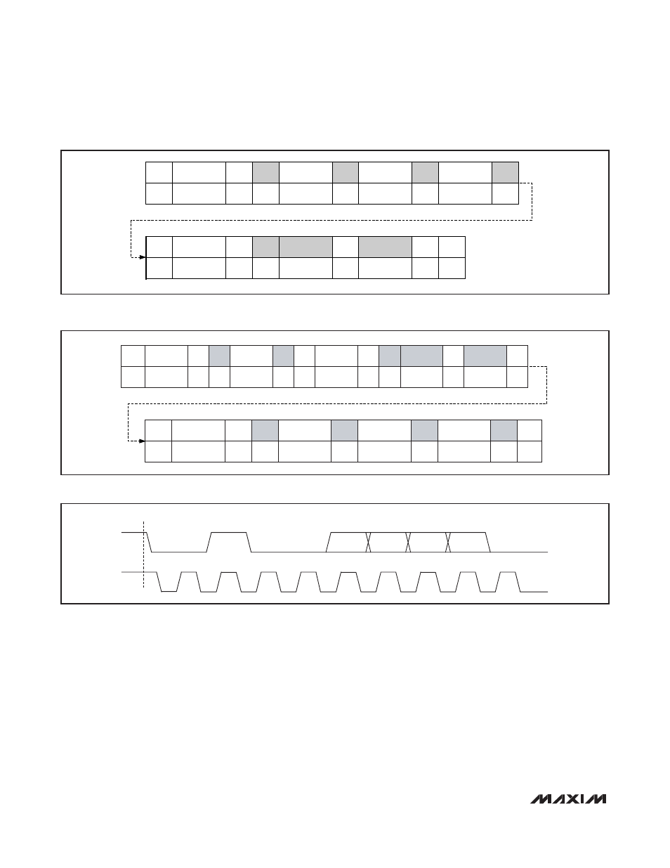
Figure 12. Write/Readback Sequence
S OR Sr
ADDRESS
ACK
READ
COMMAND
ACK
Sr
7 BITS
0
ADDRESS
DATA
ACK
DATA
Sr OR P
NACK
ACK
R/
W
8 BITS
7 BITS
8 BITS (MSB)
8 BITS (LSB)
R/
W
1
7 BITS
ADDRESS
ACK
R/
W
WRITE
COMMAND
ACK
DATA
ACK
DATA
ACK
Sr
0
8 BITS
8 BITS (MSB)
8 BITS (LSB)
Figure 13. Read-Modify-Write Sequence
SDA
SCL
0
1
0
0
A2
A1
A0
ACK
1
2
3
4
5
6
7
8
9
S
R/
W
Figure 14. Slave Address Byte