C/spi interface, Absolute maximum ratings, Electrical characteristics – Rainbow Electronics MAX1386 User Manual
Page 2
MAX1385/MAX1386
Dual RF LDMOS Bias Controllers
with I
2
C/SPI Interface
2
_______________________________________________________________________________________
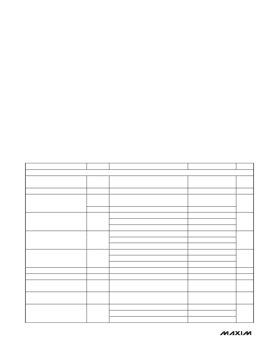
ABSOLUTE MAXIMUM RATINGS
Stresses beyond those listed under “Absolute Maximum Ratings” may cause permanent damage to the device. These are stress ratings only, and functional
operation of the device at these or any other conditions beyond those indicated in the operational sections of the specifications is not implied. Exposure to
absolute maximum rating conditions for extended periods may affect device reliability.
AV
DD
to AGND .........................................................-0.3V to +6V
DV
DD
to DGND.........................................................-0.3V to +6V
AGND to DGND.....................................................-0.3V to +0.3V
CS1+, CS1-, CS2+, CS2- to GATEGND.................-0.3V to +32V
CS1- to CS1+, CS2- to CS2+ ...................................-6V to +0.3V
GATEV
DD
to GATEGND .........................................-0.3V to +12V
GATE1, GATE2 to GATEGND ...........-0.3V to (GATEV
DD
+ 0.3V)
SAFE1, SAFE2 to GATEGND....................................-0.3V to +6V
GATEGND to AGND..............................................-0.3V to +0.3V
All Other Analog Inputs
to AGND ............-0.3V to the lower of +6V and (AV
DD
+ 0.3V)
Digital Inputs
to DGND ............-0.3V to the lower of +6V and (DV
DD
+ 0.3V)
SDA/DIN, SCL to DGND...........................................-0.3V to +6V
Digital Outputs to DGND .........................-0.3V to (DV
DD
+ 0.3V)
Maximum Continuous Current into Any Pin ........................50mA
Continuous Power Dissipation (T
A
= +70°C)
48-Pin, 7mm x 7mm, Thin QFN (derate 27.8 mW/°C
above +70°C).............................................................2222mW
Maximum Junction Temperature .....................................+150°C
Operating Temperature Range ...........................-40°C to +85°C
Storage Temperature Range .............................-65°C to +150°C
Lead Temperature (soldering, 10s) .................................+300°C
ELECTRICAL CHARACTERISTICS
(GATEV
DD
= +5.5V for the MAX1385, GATEV
DD
= +11V for the MAX1386, AV
DD
= DV
DD
= +5V, external V
REFADC
= +2.5V, external V
REF-
DAC
= +2.5V, C
REF
= 0.1µF, unless otherwise noted. T
A
= -40°C to +85°C, unless otherwise noted. Typical values are at T
A
= +25°C.)
PARAMETER
SYMBOL
CONDITIONS
MIN
TYP
MAX
UNITS
HIGH-SIDE CURRENT SENSE WITH PGA
Common-Mode Input Voltage
Range
V
CS+
, V
CS-
5
30
V
Common-Mode Rejection Ratio
CMRR
11V < V
CS+
< 30V
90
dB
I
CS+
V
SENSE
< 100mV over the common-mode
range
120
195
Input-Bias Current
I
CS-
0.002
±2
µA
PGA gain = 25
0
100
PGA gain = 10
0
250
Full-Scale Sense Voltage Range
V
SENSE
=
VCS_+ -
VCS_-
PGA gain = 2
0
1250
mV
PGA gain = 25
75
100
PGA gain = 10
75
250
Sense Voltage Range for
Accuracy of ±0.5% V
SENSE
PGA gain = 2
75
1250
mV
PGA gain = 25
20
100
PGA gain = 10
20
250
Sense Voltage Range for
Accuracy of ±2% V
SENSE
PGA gain = 2
20
1250
mV
Total PGAOUT Voltage Error
V
SENSE
= 75mV
±0.1
±0.5
%
PGAOUT Capacitive Load
C
PGAOUT
100
pF
PGAOUT Settling Time
t
HSCS
Settles to within ±0.5% of final value, R
S
=
50Ω, C
GATE
= 15pF
< 25
µs
Saturation Recovery Time
Settles to within ±0.5% accuracy; from
V
SENSE
= 3 x full scale
< 45
µs
Av
PGA
= 2
0.5
Av
PGA
= 10
2
Sense-Amplifier Slew Rate
Av
PGA
= 25
2
V/µs