C/spi interface, Table 3. th1 and th2 (read/write) – Rainbow Electronics MAX1386 User Manual
Page 28
MAX1385/MAX1386
Dual RF LDMOS Bias Controllers
with I
2
C/SPI Interface
28
______________________________________________________________________________________
IH1 and IH2 (Read/Write)
Write to Channel 1 and Channel 2 High-Current-
Threshold registers by sending the appropriate write
command byte followed by data bits D15–D0 (see
Table 5). Bits D15–D12 are don’t care. Read channel 1
and channel 2 high-current thresholds by sending the
appropriate read command byte. Channel 1 and
Channel 2 Current-Threshold registers are compared to
ADC readings at PGAOUT1 and PGAOUT2. Use the
following equation to find the required threshold code
for a specified threshold current:
where I
DRAIN
is the current threshold in amperes,
R
SENSE
is the sense resistor, Av
PGA
is the voltage gain
of the PGA, V
REFADC
is the ADC reference voltage, and
I
THRESH
is the resulting threshold register value
in decimal.
IL1 and IL2 (Read/Write)
Write to Channel 1 and Channel 2 Low-Current-
Threshold registers by sending the appropriate write
command byte followed by data bits D15–D0 (see
Table 6). Bits D15–D12 are don’t care. Read channel 1
and channel 2 low-current thresholds by sending the
appropriate read command byte. Channel 1 and
Channel 2 Low-Current Threshold registers are com-
pared to ADC readings at PGAOUT1 and PGAOUT2.
I
I
R
Av
V
THRESH
DRAIN
SENSE
PGA
REFADC
=
Ч
Ч
Ч
4096
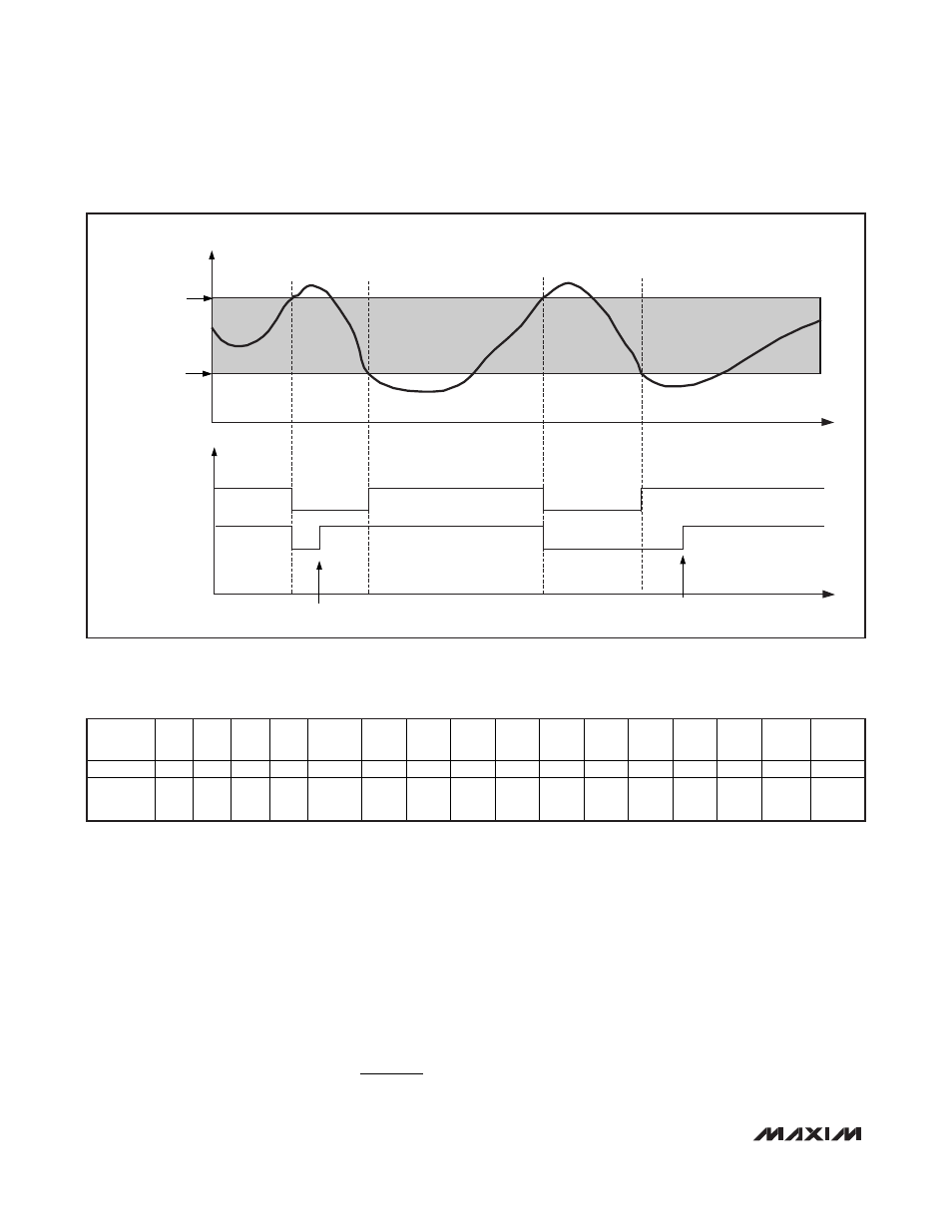
FLAG REGISTER
READ
FLAG REGISTER
READ
TIME
TIME
MEASUREMENT VALUE
(TEMPERATURE OR CURRENT)
HIGH THRESHOLD
LOW THRESHOLD
ALARM OUTPUT
OUTPUT-
COMPARATOR MODE
(ACTIVE LOW)
OUTPUT-
INTERRUPT MODE
(ACTIVE LOW)
Figure 10. Hysteresis-Threshold-Mode Timing Diagram
D15
D14
D13
D12
D11
(MSB)
D10
D9
D8
D7
D6
D5
D4
D3
D2
D1
D0
(LSB)
POR
X
X
X
X
0
1
1
1
1
1
1
1
1
1
1
1
Bit Value
(°C)
X
X
X
X
-256
+128
+64
+32
+16
+8
+4
+2
+1
+0.5
+0.25
+0.125
Table 3. TH1 and TH2 (Read/Write)
X = Don’t care.