C/spi interface – Rainbow Electronics MAX1386 User Manual
Page 44
MAX1385/MAX1386
Dual RF LDMOS Bias Controllers
with I
2
C/SPI Interface
44
______________________________________________________________________________________
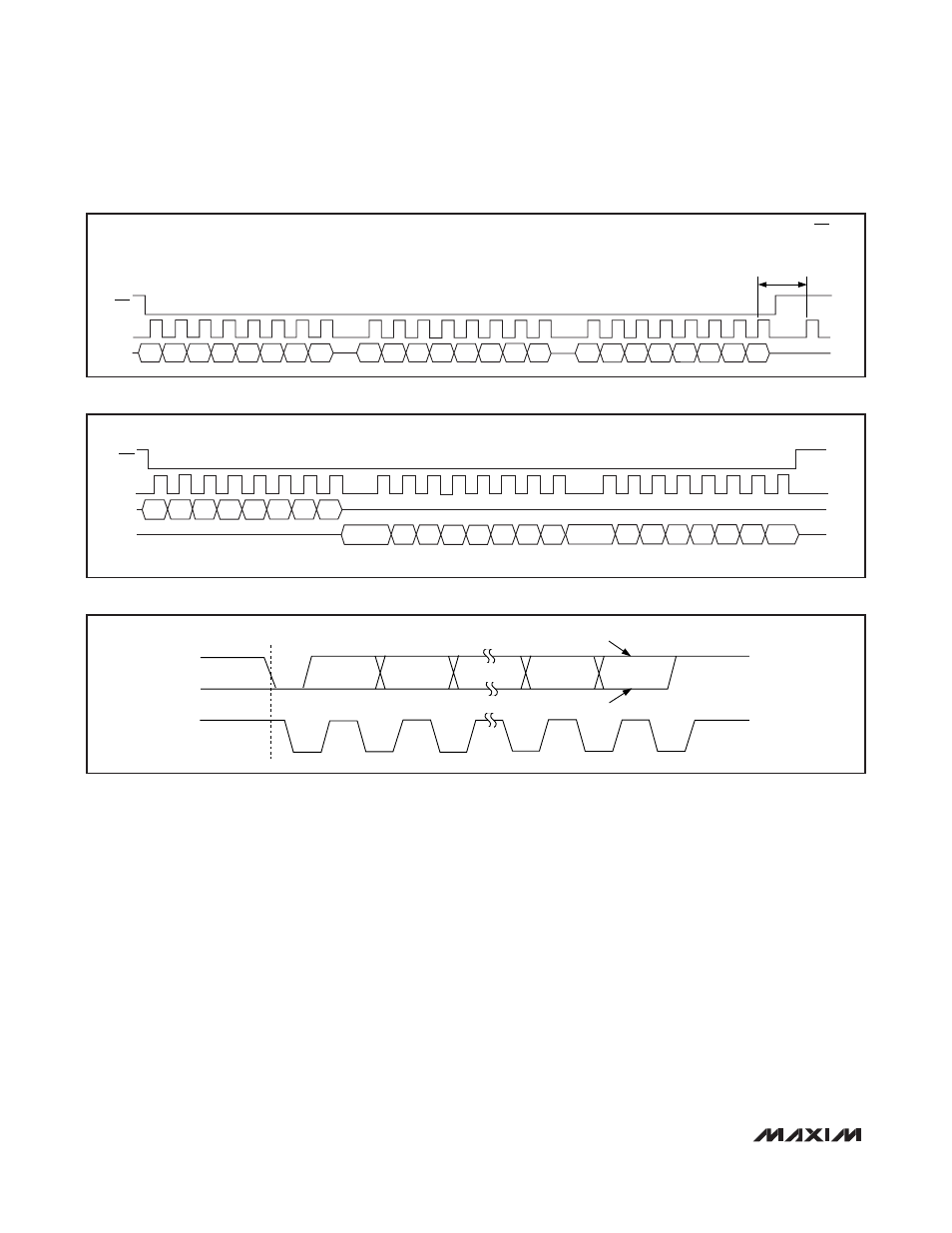
3) Send 16 bits of data (D15–D0) starting with the most
significant bit and ending with the least significant
bit. Data is clocked in on the rising edges of SCL.
4) Pull
CSB high.
Read Format
Use the following sequence to read 16 bits of data from
a MAX1385/MAX1386 register (see Figure 19):
1) Pull
CSB low to select the device.
2) Send the appropriate read command byte (see the
Command Byte
section). The command byte is
clocked in on the rising edges of SCL.
3) Receive 16 bits of data. Data is clocked out on the
falling edges of SCL.
4) Pull
CSB high.
Command Byte
The MAX1385/MAX1386 use read and write command
bytes. The command byte consists of 8 bits and contains
the address of the register (C7–C0, see Figures 18 and
19). The command byte also communicates to the
device whether a read or write operation occurs. See the
Register Description
section for details on how to access
specific registers through the command byte.
Data Bytes
Data bytes are clocked in/out of the device with the
most significant bit first and the least significant bit last
(D15–D0, see Figures 18 and 19). See the
Register
Description
section for a description of data bytes for
each register.
SCL
SDA
S
1
2
8
9
NOT ACKNOWLEDGE
ACKNOWLEDGE
Figure 20. Acknowledge Bits
SCL
C6
C5
C4
C3
C2
C1
C0
D15
D14 D13 D12
D11 D10
D9
D8
D7
D6
D5
D4
D3
D2
D1
D0
CR/W
DIN
CSB
A RISING EDGE OF CSB
DURING THIS PERIOD
COMPLETES A VALID
WRITE COMMAND.
Figure 18. SPI Write Format
SCL
C6
C5
C4
C3
C2
C1
C0
D15
D14 D13 D12 D11 D10
D9
D8
D7
D6
D5
D4
D3
D2
D1
D0
CR/W
DIN
CSB
DOUT
Figure 19. SPI Read Format