Rainbow Electronics T89C5121 User Manual
Page 9
9
A/T8xC5121
4164G–SCR–07/06
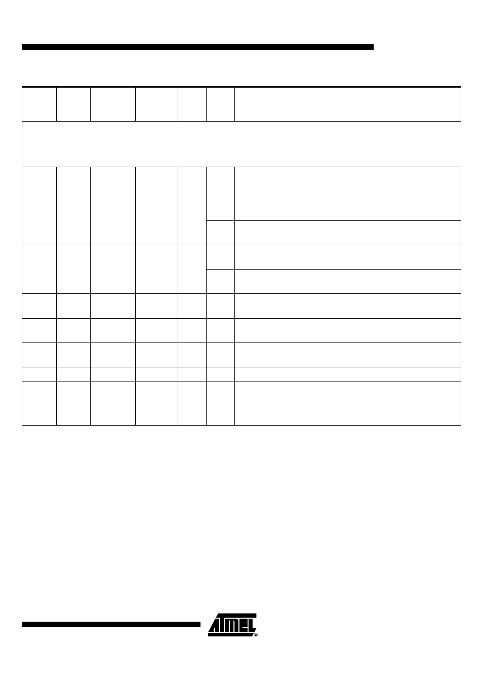
ONLY FOR PLCC52 version
P0[7:0]
AD[7:0]
V
CC
I/O
Input/Output function Port 0
P0 is an 8-bit open-drain bi-directional I/O port. Port 0 pins that
have 1s written to them float and can be used as high impedance
inputs. To avoid any parasitic current consumption, Floating P0
inputs must be pulled to V
CC
or V
SS
.
I/O
Address/Data low
Mutiplexed Address/Data LSB for external access
P2[7:0]
A[15:8]
V
CC
I/O
Input/Output function Port 2
P2 is an 8-bit open-drain bi-directional I/O port with internal pull-ups
O
Address high
Address Bus MSB for external access
P3.6
WR
DV
CC
O
Write signal
Write signal asserted during external data memory write operation
P3.7
RD
DV
CC
I
Read signal
Read signal asserted during external data memory read operation
ALE
V
CC
O
Address latch enable output
The falling edge of ALE strobes the address into external latch
PSEN
PSEN
V
CC
O
Program strobe enable
EA
EA
V
CC
I
External access enable
This pin must be held low to force the device to fetch code from
external program memory starting at address 0000h. It is latched
during reset and cannot be dynamically changed during operation.
Table 1. Ports Description (Continued)
Port
Signal
Name
Alternate
Internal
Power
Supply
ESD
Type
Description