Synchronous mode (mode 0), Transmission (mode 0), Figure 37 – Rainbow Electronics T89C5121 User Manual
Page 87
87
A/T8xC5121
4164G–SCR–07/06
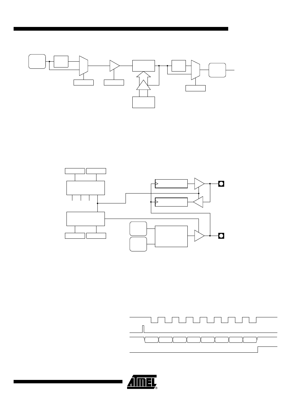
Figure 37. Internal Baud Rate Generator Block Diagram
Synchronous Mode (Mode 0)
Mode 0 is a half-duplex, synchronous mode, which is commonly used to expand the I/0
capabilities of a device with shift registers. The transmit data (TXD) pin outputs a set of
eight clock pulses while the receive data (RXD) pin transmits or receives a byte of data.
The 8-bit data are transmitted and received least-significant bit (LSB) first. Shifts occur
at a fixed Baud Rate. Figure 38 shows the serial port block diagram in Mode 0.
Figure 38. Serial I/O Port Block Diagram (Mode 0)
Transmission (Mode 0)
To start a transmission mode 0, write to SCON register clearing bits SM0, SM1.
As shown in Figure 39, writing the byte to transmit to SBUF register starts the transmis-
sion. Hardware shifts the LSB (D0) onto the RXD pin during the first clock cycle
composed of a high level then low level signal on TXD. During the eighth clock cycle the
MSB (D7) is on the RXD pin. Then, hardware drives the RXD pin high and asserts TI to
indicate the end of the transmission.
Figure 39. Transmission Waveforms (Mode 0)
0
1
Overflow
SPD
BDRCON.1
BRG
(8 bits)
BRL
(8 bits)
PER
CLOCK
÷
6
IBRG
CLOCK
BRR
BDRCON.4
0
1
SMOD1
PCON.7
÷
2
To Serial Port
BRG
CLOCK
TXD
RXD
SBUF Tx SR
SBUF Rx SR
SM1
SCON.6
SM0
SCON.7
Mode Decoder
M3 M2 M1 M0
Mode
Controller
RI
SCON.0
TI
SCON.1
PER
CLOCK
Baud Rate
Controller
Write to SBUF
TXD
RXD
TI
D0
D1
D2
D3
D4
D5
D6
D7