Spi communication—legend, Figure 23. pio read-access timing – Rainbow Electronics DS28DG02 User Manual
Page 30

DS28DG02: 2kb SPI EEPROM with PIO, RTC, Reset, Battery Monitor, and Watchdog
30 of 33
Reading from PIO
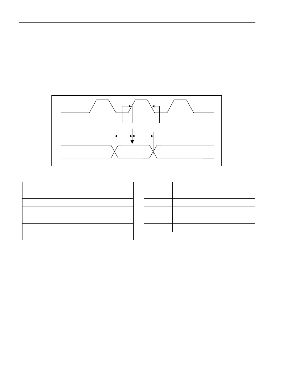
When reading from PIOs, as shown in Figure 23, the sampling is triggered by the same edge that the master uses
to clock in (read) the last data (LS) bit of the preceding byte, which may be PIO data or SRAM data. To be correctly
assessed, the PIO state must not changed during the t
PS
and t
PH
interval. The SO state is valid t
V
after the falling
edge of SCL. When reading from address 126h, the PIO state appearing first on SO is that of PIO7. With every
falling edge on SCK the next PIO state appears on SO. On the rising SCK edge after the state of PIO0 is shifted
out to SO, the PIOs of address 127h are sampled. Reading from address 127 first results in four 0-bits followed by
the state of PIO11 to PIO8. If the READ instruction is issued with starting address 126h, the DS28DG02 enters a
loop in which both groups of PIOs are read alternating between PIO0:7 and PIO8:11. This way the fastest PIO
sampling rate is f
CLK
/ 16.
Figure 23. PIO Read-Access Timing
On this edge the master
reads the LS bit of the
previous PIO data byte.
This edge shifts the MS
bit of the just sampled
PIO state to SO.
t
PS
t
PH
Sampling
SCK
PIOn
SPI Communication—Legend
SYMBOL DESCRIPTION
SYMBOL DESCRIPTION
SEL
Falling Edge on CSZ
WRITEL
Write Instruction with A8 = 0
DSEL
Rising Edge on CSZ
WRITEH
Write Instruction with A8 = 1
WREN
Write Enable Instruction
READL
Read Instruction with A8 = 0
WRDI
Write Disable Instruction
READH
Read Instruction with A8 = 1
WRSR
Write Status Register Instruction
Transfer of 1 Byte
RFSH Refresh
Instruction
