Rainbow Electronics DS28DG02 User Manual
Page 29
DS28DG02: 2kb SPI EEPROM with PIO, RTC, Reset, Battery Monitor, and Watchdog
29 of 33
Figure 21. PIO Write Access Timing, Low-Current Mode
This edge clocks in the last (LS)
bit of the new PIO data byte.
This edge starts the
transfer of the new data to
the PIO pins. See Note.
t
OT
SCK
PIOn
The t
OT
timing reference is 80%
or 20% of maximum current.
Note
: In SPI Mode (1,1) there is no falling SCK edge for the last bit of the last byte sent to the device; in this case,
the transfer to the PIO is initiated with the rising edge of CSZ. This note also applies to the high-current mode.
Writing in High-Current Mode
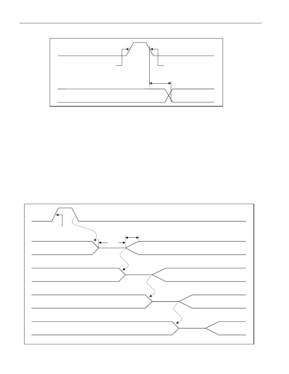
When writing to PIOs in high-current mode, the state change is triggered by the falling edge of SCK after the last bit
of the new PIO state is shifted into the DS28DG02. The PIOs change their state sequentially, as shown in Figure
22, beginning with PIO0 or PIO8, respectively, depending on the address. A PIO that is changing its state is first tri-
stated for 2µs maximum. This 2µs delay also applies to PIOs configured as input and to PIOs configured as output
that do not change their state. The state transition of PIOs in high-current mode is slew-rate controlled to prevent
immediate full current-drive or release. Each pin’s slew-rate circuit is designed to ramp up to the full current drive or
release over the course of 1μs. The t
OT
value specified for high-current mode is valid when updating all 12 PIOs in
a single write access. In this case there is an extra 1µs maximum delay when transitioning from PIO7 to PIO8. In
high-current mode, the automatic alternation between groups of PIOs does not apply; another WREN and WRITE
sequence is necessary to update the PIO states again.
Figure 22. PIO Write Access Timing, High-Current Mode
This edge clocks in the last (LS)
bit of the new PIO data byte.
SCK
PIO0 (PIO8)
PIO1 (PIO9)
PIO2 (PIO10)
PIO3 (PIO11)
2µs
max.
1µs max.
Tri-stated