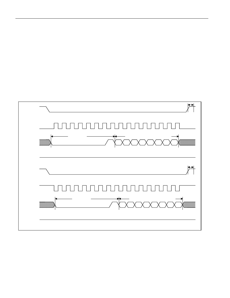
Wrsr write spi status register, Figure 15. write spi status register timing, Csz sck si so – Rainbow Electronics DS28DG02 User Manual
Page 22: Rdsr read spi status register

DS28DG02: 2kb SPI EEPROM with PIO, RTC, Reset, Battery Monitor, and Watchdog
22 of 33
WRSR Write SPI Status Register
The WRSR instruction is the only way to update the nonvolatile bits (b7:b2) of the SPI Status register. See Figure
12 for a detailed description of the nonvolatile bits and their function. As a precondition for a successful write
access to the Status register, the WEN bit must be 1 and either the WPEN bit must be 0, or both WPEN and the
logic state at the WPZ pin must be 1, as shown in the write protection summary of Table 2. The WEN bit is set
through the WREN instruction, which must be completed before any write instruction. The WRSR timing diagram
for both SPI communication modes is shown in Figure 15. The graphic assumes that only a single byte follows the
instruction code. In case of multiple bytes following the instruction code, the last of these data bytes is used to
update the SPI Status register. If the SPI Status register is not write-protected AND the WEN bit 1, the write cycle
(transfer to EEPROM) begins with the positive edge of CSZ. The duration of the write cycle is t
PROG
, during which
the RDYZ bit of the SPI Status register reads 1. After the write cycle is completed, the WEN bit is cleared. If the
SPI Status register is write-protected OR WEN was not set to 1 before issuing the WRSR instruction, the positive
edge on CSZ does not start a write cycle and the WEN bit is not cleared. The first Read Memory sequence
executed after WRSR always delivers data from addresses 100h and higher, regardless of the address bit in the
instruction code.
Figure 15. Write SPI Status Register Timing
0 1 2 3 4 5 6 7 8 9 10 11
12
13 14 15
CSZ
SCK
SI
SO
High Impedance
Write Status, Mode (0,0)
0 0 0 0 0 0 0 1 7 6 5 4 3 2 1 0
Instruction
Data to SPI Status Register
t
PROG
0 1 2 3 4 5 6 7 8 9 10
11 12
13
14 15
CSZ
SCK
SI
SO
High Impedance
Write Status, Mode (1,1)
0 0 0 0 0 0 0 1 7 6 5 4 3 2 1 0
Instruction
Data to SPI Status Register
t
PROG
RDSR Read SPI Status Register
RDSR is the only instruction that the DS28DG02 accepts and executes at any time, even if an EEPROM write
cycle is in progress. See Figure 12 for a detailed description of the SPI Status register bits. Besides providing
general read access to the SPI Status register, the main use of this instruction is for the master to test the RDYZ
bit, which signals the end of an EEPROM write cycle. Figure 16 shows the RDSR timing diagram for both SPI
communication modes. The RDYZ state reported through the RDSR instruction is updated on the negative edge of
SCK during the transmission of the LS-bit of the status byte (highlighted in Figure 16, the Mode (0,0) 16 clock
cycles graphic). This allows the master to repeatedly read the SPI Status register by generating additional SCK
pulses, without having to resend the instruction code. The RDSR instruction ends with the positive edge on CSZ.
