Rainbow Electronics DS28DG02 User Manual
Page 27

DS28DG02: 2kb SPI EEPROM with PIO, RTC, Reset, Battery Monitor, and Watchdog
27 of 33
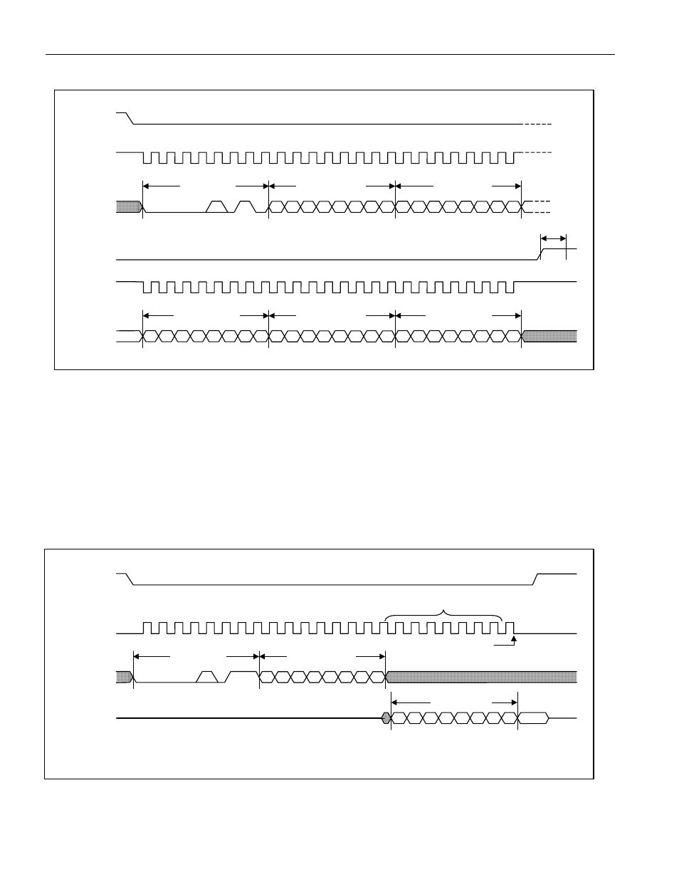
Figure 19. Multiple-Byte Write to Memory and PIO Timing (continued)
CSZ
SCK
SI
Multiple-Byte Write Timing, Mode (1,1)
0 1 2 3 4 5 6 7 8 9 10 11 12 13 14 15 16 17 18 19 20 21 22 23
0 0 0 0 A8 0 1 0 7 6 5 4 3 2 1 0 7 6 5 4 3 2 1 0
Instruction
8-bit Address
Data Byte 1
CSZ
SCK
SI
7 6 5 4 3 2 1 0 7 6 5 4 3 2 1 0 7 6 5 4 3 2 1 0
Data Byte n-2
Data Byte n-1
Data Byte n
t
PROG
Read Memory and PIO
The read timing diagram for both SPI communication modes is shown in Figure 20. The read-access timing is
independent of the addressed memory type. Upon receiving a read instruction with an address in the range of 000h
to 135h the DS28DG02 transmits data, first the SPI Status register value and then data from the specified target
address. Addresses marked “reserved” read 00h. The address pointer increments with every data byte transmitted
to the master. After data from address 135h is read, the address pointer wraps around to 000h. The master may
continue reading data bytes indefinitely. The read access ends with the positive edge on CSZ. If prior to the Read
Memory and PIO sequence a WRSR command was executed, the address bit embedded in the instruction code is
ignored and data is delivered from addresses 100h and higher. The application firmware should include a
command such as WRDI after WRSR to ensure reading from the intended address.
Figure 20. Read Memory and PIO Timing
CSZ
SCK
SI
SO
High Impedance
0 1 2 3 4 5 6 7 8 9 10 11 12 13 14 15
Read Timing, Mode (0,0)
0 0 0 0 A8 0 1 1 7 6 5 4 3 2 1 0
Instruction
8-bit Address
Data Byte
1)
7 6 5 4 3 2 1 0 7
8 Falling Edges for Each Data Byte
Note: This edge ends the LS bit (0) of the previous byte and begins the MS bit (7) of the next byte.
See Note
1)
The first byte delivered by the device is the SPI Status Byte. After that the memory data follows.
