Rainbow Electronics W27E010 User Manual
General description, Features, Pin configurations

W27E010
128K
×
8 ELECTRICALLY ERASABLE EPROM
Publication Release Date: May 1997
- 1 -
Revision A5
GENERAL DESCRIPTION
The W27E010 is a high speed, low power Electrically Erasable and Programmable Read Only
Memory organized as 131072
×
8 bits that operates on a single 5 volt power supply. The W27E010
provides an electrical chip erase function.
FEATURES
•
High speed access time:
45/55/70/90/120 nS (max.)
•
Read operating current: 30 mA (typ.)
•
Erase/Programming operating current:
1 mA (typ.)
•
Standby current: 5
µ
A (typ.)
•
Single 5V power supply
•
+14V erase/+12V programming voltage
•
Fully static operation
•
All inputs and outputs directly TTL/CMOS
compatible
•
Three-state outputs
•
Available
packages: 32-pin 600 mil DIP, 450
mil SOP and PLCC
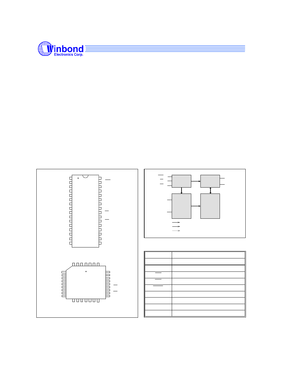
PIN CONFIGURATIONS
A6
A5
A4
A3
A2
A1
A0
Q0
5
6
7
8
9
10
11
12
13
Q
1
Q
2
Q
4
Q
5
Q
6
1
4
4
3 2
1
3
2
3
1
3
0
A14
A13
A8
A9
OE
A11
Q7
29
28
27
26
25
24
23
22
21
32-pin PLCC
G
N
D
1
5
1
6
1
7
1
8
1
9
2
0
N
C
V
c
c
CE
A10
Q5
OE
A10
Q7
Q6
A13
A8
A9
A11
PGM
NC
Q0
A0
A2
A3
A4
A5
A6
A7
A12
A15
A16
A14
A1
Vcc
Vpp
A
1
5
A
1
6
1
2
3
4
5
6
7
8
9
10
11
12
13
14
15
16
30
31
32
25
26
27
28
29
20
21
22
23
24
19
18
17
Q3
Q4
GND
Q2
CE
Q1
Q
3
A7
A
1
2
V
p
p
/
P
G
M
BLOCK DIAGRAM
CONTROL
OUTPUT
BUFFER
DECODER
CORE
ARRAY
Q0
Q7
.
.
CE
OE
A0
.
.
V
GND
CC
A16
PGM
V
PP
PIN DESCRIPTION
SYMBOL
DESCRIPTION
A0
−
A16
Address Inputs
Q0
−
Q7
Data Inputs/Outputs
CE
Chip Enable
OE
Output Enable
PGM
Program Enable
V
PP
Program/Erase Supply Voltage
V
CC
Power Supply
GND
Ground
NC
No Connection
FUNCTIONAL DESCRIPTION
