Rainbow Electronics DS28DG02 User Manual
Page 11

DS28DG02: 2kb SPI EEPROM with PIO, RTC, Reset, Battery Monitor, and Watchdog
11 of 33
PIO Read Access
ADDR
b7 b6 b5 b4 b3 b2 b1 b0
126h
IV7 IV6 IV5 IV4 IV3 IV2 IV1 IV0
127h
0 0 0 0
IV11
IV10
IV9
IV8
There is only read access to these addresses. Bits 4 to 7 of address 127h always read 0. Read access is functional
for all PIOs, regardless of their direction setting. Reported is the logic state of the pin, which may be different from
what the PIO output value register implies.
BIT DESCRIPTION
BIT(S)
DEFINITION
IVn: Input Value of PIOn
—
Logic state read from PIO0 to PIO11 pins. IV0 applies to PIO0, etc.
Legend
:
IVn = PIOn XOR’ed with IMSKn
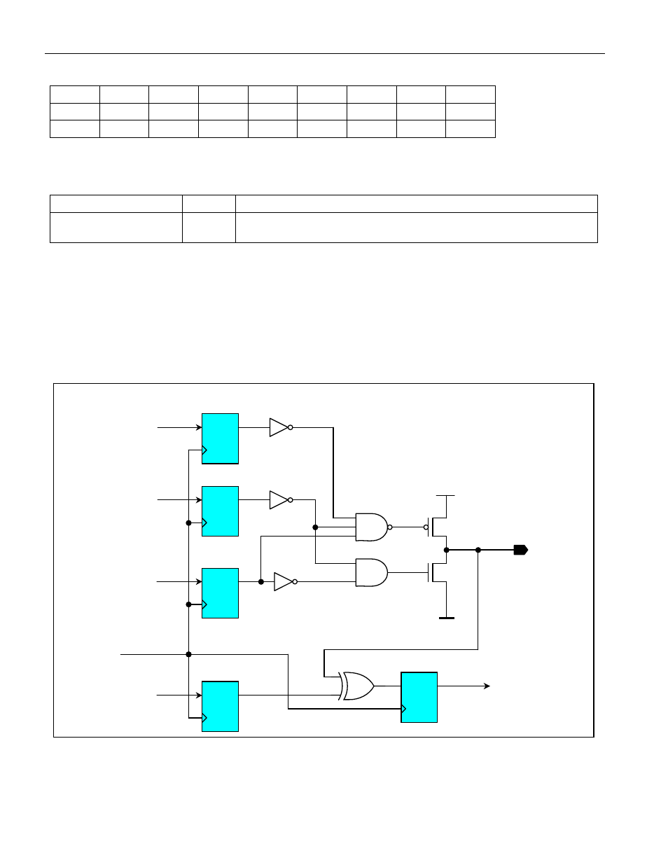
Figure 4 shows a simplified schematic of a PIO. The flip flops are accessed through the PIO Output State (OVn)
and Read Access (IVn) registers and memory addresses 122h to 125 (DIRn, IMSKn, OTn). They are initialized at
power-up or during Refresh (see the SPI Interface Description) according to the data stored at memory addresses
10Ah to 10Fh. When a PIO is configured as input, the PIO output is tri-stated (high impedance). When a PIO is
configured as output, the PIO input is the same as the output state XORed with the corresponding read inversion
bit. The differences of the PIO behavior in low current and high current mode are explained in the PIO Read/Write
Access
section near the end of this document.
Figure 4. PIO Simplified Schematic
D Q
CLK
D Q
CLK
D Q
CLK
D Q
CLK
DIRn
OVn
OTn
Vcc
D Q
CLK
IMSKn
PIOn Pin
to SPI Interface
IVn
OTn
from SPI Interface
CLK
DIRn
from SPI Interface
OVn
from SPI Interface
IMSKn
from SPI Interface
