Rainbow Electronics AT27LV040A User Manual
Features, Description, Pin configurations
1
Features
•
Fast Read Access Time - 90 ns
•
Dual Voltage Range Operation
– Low Voltage Power Supply Range, 3.0V to 3.6V
or Standard 5V
±
10% Supply Range
•
Compatible With JEDEC Standard AT27C040
•
Low Power 3.3-volt CMOS Operation
– 20 µA max. (less than 1 µA typical) Standby for V
CC
= 3.6V
– 36 mW max. Active at 5 MHz for V
CC
= 3.6V
•
JEDEC Standard Packages
– 32-Lead PLCC
– 32-Lead TSOP (8 x 20 mm)
– 32-Lead VSOP (8 x 14 mm)
•
High Reliability CMOS Technology
– 2,000V ESD Protection
– 200 mA Latchup Immunity
•
Rapid™ Programming Algorithm - 100 µs/byte (typical)
•
CMOS and TTL Compatible Inputs and Outputs
– JEDEC Standard for LVTTL
•
Integrated Product Identification Code
•
Commercial and Industrial Temperature Ranges
Description
The AT27LV040A is a high performance, low power, low voltage, 4,194,304-bit one-
time programmable read only memory (OTP EPROM) organized as 512K by 8 bits. It
requires only one supply in the range of 3.0 to 3.6V in normal read mode operation,
making it ideal for fast, portable systems using battery power.
Atmel’s innovative design techniques provide fast speeds that rival 5V parts while
keeping the low power consumption of a 3V supply. At V
CC
= 3.0V, any byte can be
accessed in less than 90 ns. With a typical power dissipation of only 18 mW at 5 MHz
and V
CC
= 3.3V, the AT27LV040A consumes less than one half the power of a stan-
dard 5V EPROM. Standby mode supply current is typically less than 1
µ
A at 3.3V.
4-Megabit
(512K x 8)
Low Voltage
OTP EPROM
AT27LV040A
Rev. 0557B–10/98
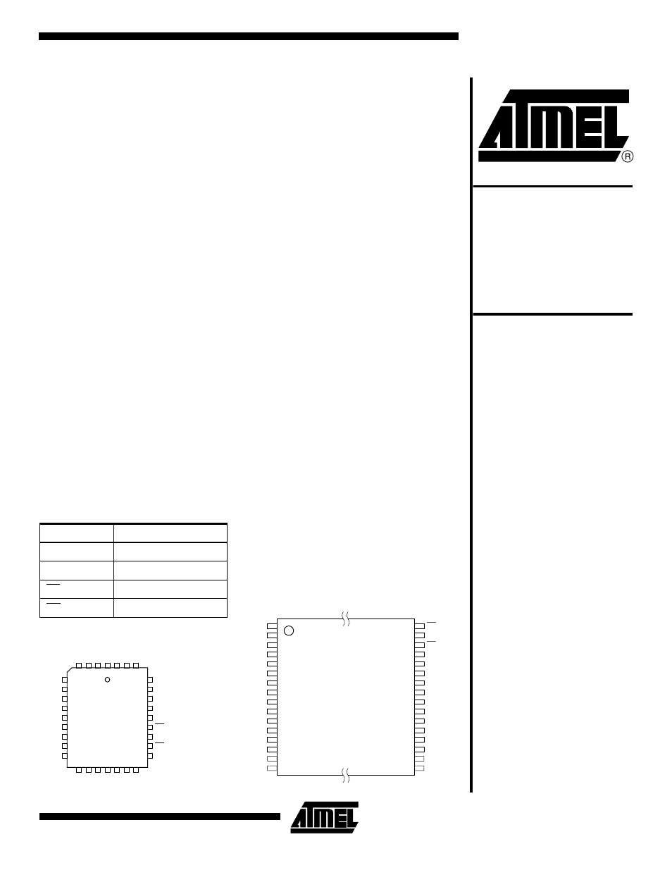
Pin Configurations
Pin Name
Function
A0 - A18
Addresses
O0 - O7
Outputs
CE
Chip Enable
OE
Output Enable
TSOP, VSOP Top View
Type 1
1
2
3
4
5
6
7
8
9
10
11
12
13
14
15
16
32
31
30
29
28
27
26
25
24
23
22
21
20
19
18
17
A11
A9
A8
A13
A14
A17
A18
VCC
VPP
A16
A15
A12
A7
A6
A5
A4
OE
A10
CE
O7
O6
O5
O4
O3
GND
02
01
O0
A0
A1
A2
A3
PLCC Top View
5
6
7
8
9
10
11
12
13
29
28
27
26
25
24
23
22
21
A7
A6
A5
A4
A3
A2
A1
A0
O0
A14
A13
A8
A9
A11
OE
A10
CE
O7
4
3
2
1
32
31
30
14
15
16
17
18
19
20
O1
O2
GND
O3
O4
O5
O6
A12
A15
A16
VPP
VCC
A18
A17
(continued)