Rfsh refresh pio registers, Figure 17. refresh pio registers timing, Table 3. write access cases – Rainbow Electronics DS28DG02 User Manual
Page 24

DS28DG02: 2kb SPI EEPROM with PIO, RTC, Reset, Battery Monitor, and Watchdog
24 of 33
RFSH Refresh PIO Registers
The volatile PIO-related registers from address 120h to 125h are preset with their power-on default values stored in
EEPROM when the device powers up. The fastest way for the master to restore the power-on state without power-
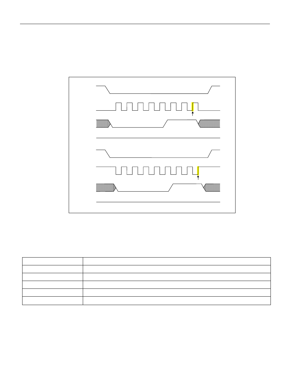
cycling the DS28DG02 is through the RFSH instruction. The RFSH timing diagram for both SPI communication
modes is shown in Figure 17. The PIO register restore begins when the last bit of the instruction code is clocked
into the device (highlighted SCK transition) and ends after the power-up wait time (t
POIP
) is over.
Figure 17. Refresh PIO Registers Timing
0 0 0 0 0 1 1 1
0 1 2 3 4 5 6 7
CSZ
SCK
SI
SO
High Impedance
Refresh, Mode (0,0)
0 1 2 3 4 5 6 7
CSZ
SCK
SI
SO
0 0 0 0 0 1 1 1
High Impedance
Refresh, Mode (1,1)
WRITE Write to Memory and PIO
From the perspective of the master, the DS28DG02 is a memory device with memory ranges made of EEPROM,
SRAM and ROM. Depending on the memory type, the behavior of the device upon receiving a write instruction
varies. Table 3 shows the cases that need to be distinguished.
Table 3. Write Access Cases
STARTING ADDRESS
DESCRIPTION
000h to 0FFh
User memory (can be write-protected through BP1:BP0).
100h to 10Fh
EEPROM registers (reserved and power-on default values, no write-protection).
110h to 11Fh
Read-only memory.
120h to 135h
SRAM, PIO, and NV SRAM (may be write-protected through RPROT).
136h to 1FFh
Nonexisting memory.
The four blocks of user memory consist of 16 segments of 16 bytes each. The first segment begins at address
000h and ends at address 00Fh; segment 2 ranges from 010h to 01Fh, etc. Upon receiving a write instruction with
an address targeting the user memory, any data bytes that follow the address are written to a 16-byte buffer,
beginning at an offset that is determined by the 4 least significant bits of the target address. This buffer is initialized
(pre-loaded) with data from the addressed 16-byte EEPROM segment. Incoming data replaces pre-loaded data.
With every byte received, the buffer's write pointer is incremented. This allows updating from 1 to 16 bytes starting
anywhere within the segment. If the write pointer has reached its maximum value of 1111b and additional data is
received, the pointer wraps around (rolls over) and the incoming data is written to the beginning of the EEPROM
write buffer and continuing. If the target memory is not write-protected AND the WEN bit of the SPI Status register
