Rainbow Electronics AT45DB011B User Manual
Megabit 2.7-volt only dataflash, Features, Description
1
1-megabit
2.7-volt Only
DataFlash
®
AT45DB011B
Features
•
Single 2.7V - 3.6V Supply
•
Serial Peripheral Interface (SPI) Compatible
•
20 MHz Max Clock Frequency
•
Page Program Operation
– Single Cycle Reprogram (Erase and Program)
– 512 Pages (264 Bytes/Page) Main Memory
•
Supports Page and Block Erase Operations
•
One 264-byte SRAM Data Buffer
•
Continuous Read Capability through Entire Array
– Ideal for Code Shadowing Applications
•
Fast Page Program Time – 7 ms Typical
•
120 µs Typical Page to Buffer Transfer Time
•
Low Power Dissipation
– 4 mA Active Read Current Typical
– 2 µA CMOS Standby Current Typical
•
Hardware Data Protection Feature
•
100% Compatible with AT45DB011
•
Commercial and Industrial Temperature Ranges
Description
The AT45DB011B is a 2.7-volt only, serial interface Flash memory ideally suited for
a wide variety of digital voice-, image-, program code- and data-storage applications.
Its 1,081,344 bits of memory are organized as 512 pages of 264 bytes each. In addi-
tion to the main memory, the AT45DB011B also contains one SRAM data buffer of 264
bytes. The buffer allows receiving of data while a page in the main memory is being
reprogrammed. EEPROM emulation (bit or byte alterability) is easily handled with a
self-contained three step Read-Modify-Write operation. Unlike conventional Flash
memories that are accessed randomly with multiple address lines and a parallel inter-
face, the DataFlash uses a SPI serial interface to sequentially access its data. SPI
mode 0 and mode 3 are supported. The simple serial interface facilitates hardware
AT45DB011B
Preliminary 16-
Megabit 2.7-volt
Only Serial
DataFlash
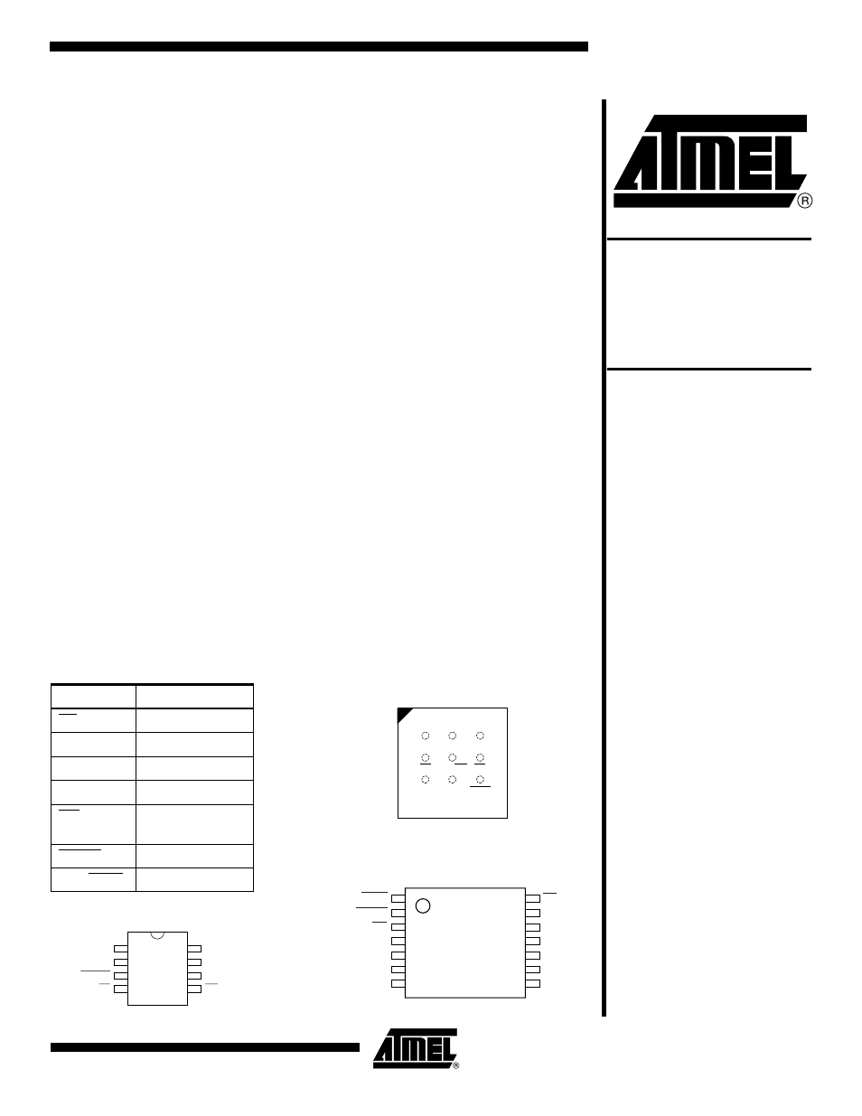
Pin Configurations
Pin Name
Function
CS
Chip Select
SCK
Serial Clock
SI
Serial Input
SO
Serial Output
WP
Hardware Page
Write Protect Pin
RESET
Chip Reset
RDY/BUSY
Ready/Busy
CBGA Top View
through Package
A
B
C
1
2
3
VCC
WP
RESET
GND
RDY/BSY
SI
SCK
CS
SO
TSSOP Top View
Type 1
1
2
3
4
5
6
7
14
13
12
11
10
9
8
RDY/BUSY
RESET
WP
VCC
GND
SCK
SO
CS
NC
NC
NC
NC
NC
SI
SOIC
1
2
3
4
8
7
6
5
SI
SCK
RESET
CS
SO
GND
VCC
WP
Rev. 1984E–DFLSH–10/02
Document Outline
- Pin Configurations
- Features
- Description
- Block Diagram
- Memory Array
- Memory Architecture Diagram
- Device Operation
- Status Register Format
- Block Erase Addressing
- Additional Commands
- Absolute Maximum Ratings*
- DC and AC Operating Range
- Power-on/Reset State
- System Considerations
- DC Characteristics
- AC Characteristics
- Input Test Waveforms and Measurement Levels
- Output Test Load
- AC Waveforms
- Write Operations
- Read Operations
- Detailed Bit-level Read Timing – Inactive Clock Polarity Low
- Detailed Bit-level Read Timing – Inactive Clock Polarity Low (Continued)
- Detailed Bit-level Read Timing – Inactive Clock Polarity High
- Detailed Bit-level Read Timing – Inactive Clock Polarity High (Continued)
- Detailed Bit-level Read Timing – SPI Mode 0
- Detailed Bit-level Read Timing – SPI Mode 0 (Continued)
- Detailed Bit-level Read Timing – SPI Mode 3
- Detailed Bit-level Read Timing – SPI Mode 3 (Continued)
- Sector Addressing
- Ordering Information
- Packaging Information