Csz sck si so, Pio read/write access – Rainbow Electronics DS28DG02 User Manual
Page 28
DS28DG02: 2kb SPI EEPROM with PIO, RTC, Reset, Battery Monitor, and Watchdog
28 of 33
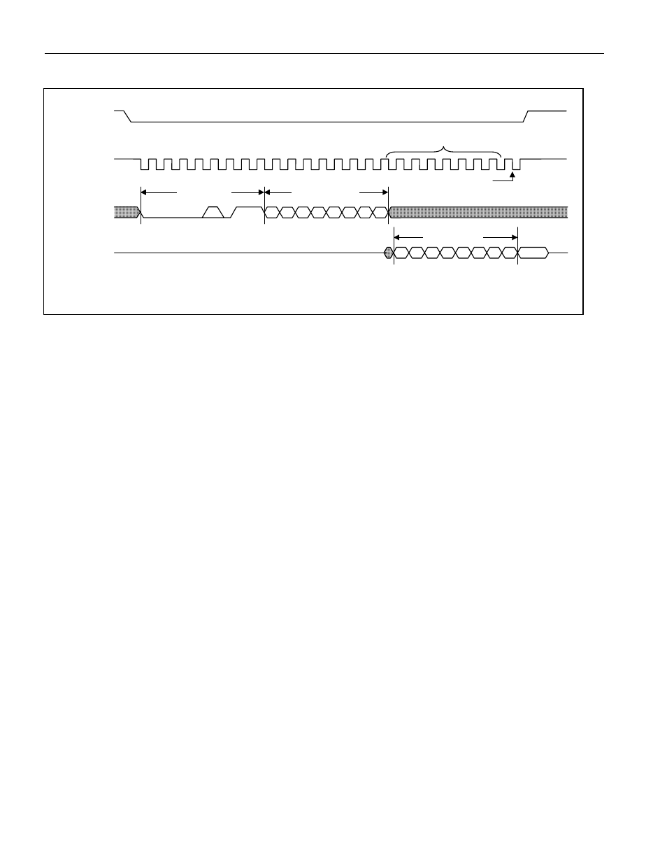
Figure 20. Read Memory and PIO Timing (continued)
CSZ
SCK
SI
SO
Read Timing, Mode (1,1)
High Impedance
7 6 5 4 3 2 1 0 7
0 1 2 3 4 5 6 7 8 9 10 11
12 13 14 15
8 Falling Edges for Each Data Byte
0 0 0 0 A8 0 1 1 7 6 5 4 3 2 1 0
Instruction
8-bit Address
See Note
Note: This edge ends the LS bit (0) of the previous byte and begins the MS bit (7) of the next byte.
Data Byte
1)
1)
The first byte delivered by the device is the SPI Status Byte. After that the memory data follows.
When reading the
RTC
and Calendar registers, the data reported to the master is taken from a buffer. This buffer is
loaded when the least significant address bit is transmitted during a READ instruction. This buffer is not updated
between bytes or when the address pointer wraps around. If the starting target address specified after the
instruction code points to the PIO Read Access registers (address 126h or 127h) the address pointer toggles
between 126h or 127h after a data byte is transmitted. This allows fast PIO reads, e.g., to monitor several signals.
For a PIO-read timing diagram see the PIO Read/Write Access section.
If a read instruction requests data from nonexisting memory, the DS28DG02 initially transmits 00h bytes until the
address pointer eventually changes to 000h. Subsequently, the device transmits valid data and the read pointer
increments normally, wrapping around to 000h after having reached 135h.
PIO Read/Write Access
General Information
When the DS28DG02 powers up, the PIO direction, output state, output type, output mode, and read-inversion are
set automatically from power-on default values stored in EEPROM. The duration of this initialization phase is t
POIP
,
during which each PIO is temporarily set as input with the output driver tri-stated to prevent conflicts with circuitry
connected to the PIO pins. The output drivers of PIOs that are configured as input are tri-stated (high impedance).
The PIO output drivers of the DS28DG02 are designed to deliver high currents for driving LEDs or similar loads.
Switching multiple PIOs conducting high current simultaneously could errantly trigger the reset monitor circuit. To
prevent this from happening, it is necessary to set the OTM bit at address 125h, which activates the high-current
mode where the PIO channels switch sequentially. In high-current mode changes in direction or output type do not
take effect immediately; they are delayed until the next PIO write access when the associated bit transition is
evaluated. Since writing to PIOs is a write function, the WEN bit must be set before issuing the WRITE instruction.
Writing in Low-Current Mode
When writing to PIOs in low-current mode, as shown in Figure 21, any state change is triggered by the falling edge
of SCK after the last bit of the new PIO state is shifted into the DS28DG02. All addressed PIOs (8 with address
120h or 4 with address 121h) change their state approximately at the same time. After the output transition time t
OT
is expired, the state change is completed. If the WRITE instruction is issued with starting address 120h, the
DS28DG02 enters a loop in which incoming data is directed to both groups of PIOs alternating between PIO0:7
and PIO8:11. This way the fastest rate for a PIO to change its state is f
CLK
/ 16.