Rainbow Electronics W27L520 User Manual
General description, Features, Pin configurations

Preliminary W27L520
64K
××
8 ELECTRICALLY ERASABLE EPROM
Publication Release Date: 4/26/2000
- 1 -
Revision A2
GENERAL DESCRIPTION
The W27L520 is a high speed, low power Electrically Erasable and Programmable Read Only
Memory organized as 65,536
×
8 bits. It includes latches for the lower 8 address lines to multiplex
with the 8 data lines. To cooperate with the MCU, this device could save the external TTL
component, also cost and space. It requires only one supply in the range of 3.0V in normal read
mode. The W27L520 provides an electrical chip erase function. It will be a great convenient when you
need to change/update the contents in the device.
FEATURES
•
High speed access time: 70/90 nS (max.)
•
Read operating current: 8 mA (max.)
•
Erase/Programming operating current
30 mA (max.)
•
Standby current: 20
µ
A (max.)
•
Unregulated battery power supply range,
3.0V to 3.6V
•
+13V erase and programming voltage
•
High Reliability CMOS Technology
- 2K V ESD Protection
- 200 mA Latchup Immunity
•
Fully static operation
•
All inputs and outputs directly LVTTL/CMOS
compatible
•
Three-state outputs
•
Available p
ackages: 20-pin TSSOP and 20-pin
SOP
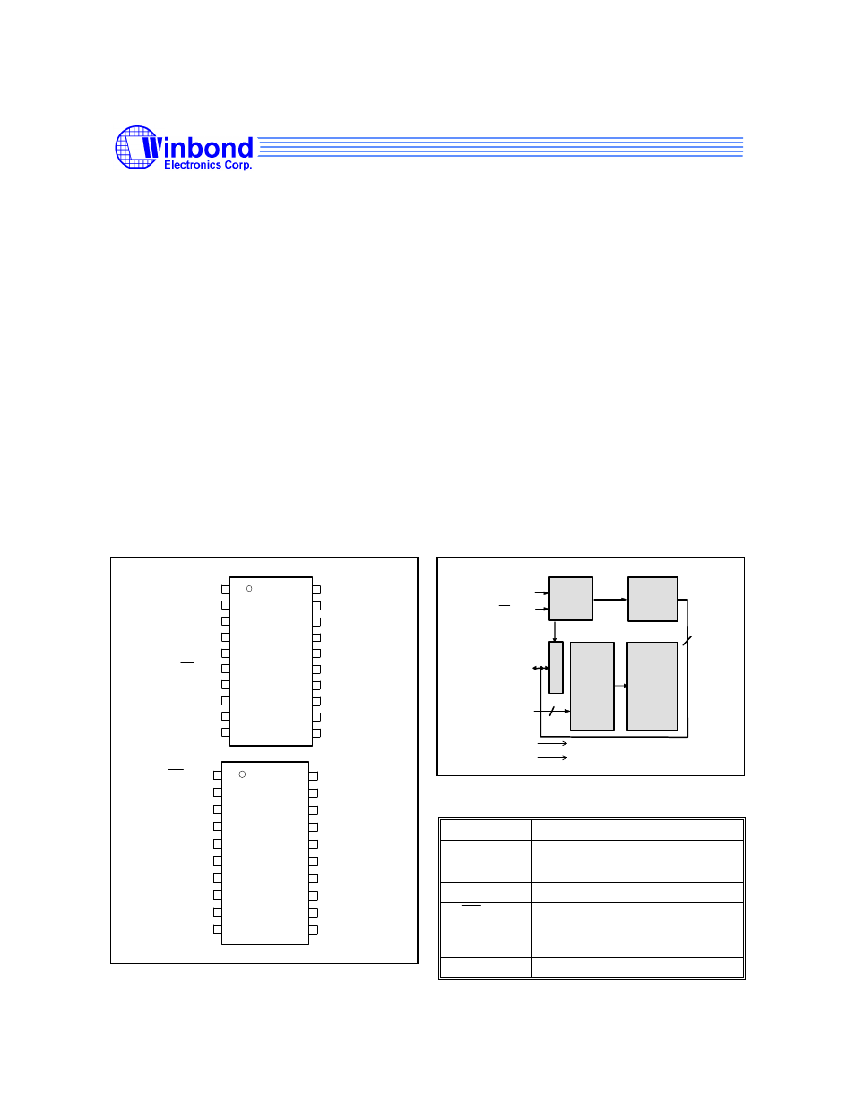
PIN CONFIGURATIONS
1
2
3
4
5
6
7
8
18
19
20
13
14
15
16
17
11
12
9
10
AD2
AD0
AD7
GND
AD6
AD4
AD1
AD3
AD5
A9
A11
A13
A15
OE/VPP
ALE
A14
A12
V
DD
TSSOP
Top View
A10
A8
18
19
20
1
2
3
4
5
6
7
8
13
14
15
17
11
12
9
10
AD5
AD0
A10
A8
AD1
AD3
ALE
A14
A12
GND
AD6
AD4
AD2
A11
A13
A15
SOP
Top View
A9
OE/VPP
VDD
AD7
16
BLOCK DIAGRAM
ALE
OE / V
CONTROL
GND
V
DD
PP
AD7 - AD0
OUTPUT
BUFFER
DECODER
L
A
T
C
H
E
S
A15 - A8
MEMORY
ARRAY
PIN DESCRIPTION
SYMBOL
DESCRIPTION
AD0
−
AD7
Address/Data Inputs/Outputs
A8
−
A15
Address Inputs
ALE
Address Latch Enable
OE /V
PP
Output Enable, Program/Erase
Supply Voltage
V
DD
Power Supply
GND
Ground
