Figure 6-5, Method 2, Chapter 6: the ten-bit interface – Xilinx 1000BASE-X User Manual
Page 74
74
Ethernet 1000BASE-X PCS/PMA or SGMII v9.1
UG155 March 24, 2008
Chapter 6: The Ten-Bit Interface
R
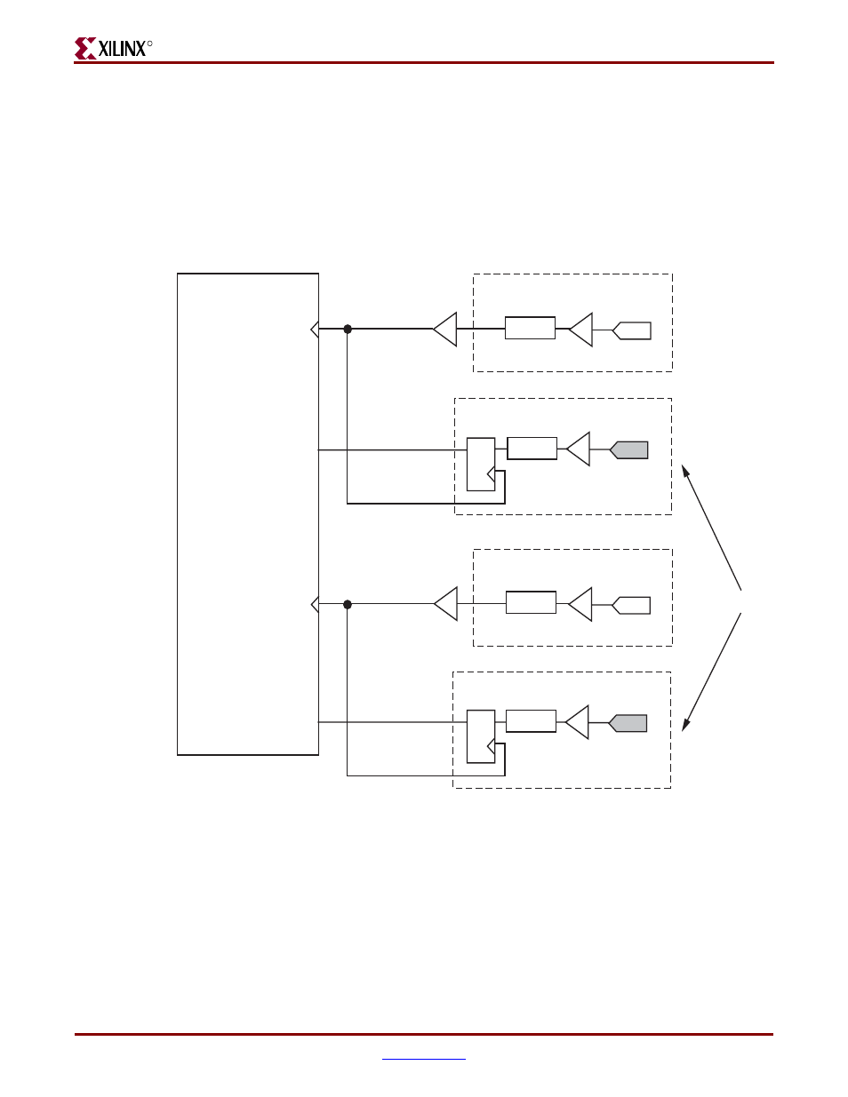
Method 2
This logic from method 1 relies on pma_rx_clk0 and pma_rx_clk1 being exactly 180
degrees out of phase with each other since the falling edge of pma_rx_clk0 is used in
place of pma_rx_clk1. See the data sheet for the attached SERDES to verify that this is the
case. If not, then the logic of
illustrates an alternative implementation where
both pma_rx_clk0 and pma_rx_clk1 are used as intended. Each bit of
rx_code_group[9:0]
must be routed to two separate device pads.
Figure 6-5:
Alternate Ten-Bit Interface Receiver Logic for Virtex-4 Devices
pma_rx_clk0
IBUFG
IOB LOGIC
IPAD
rx_code_group[0]
IBUF
IPAD
Ethernet 1000BASE-X PCS/PMA
or SGMII LogiCORE
pma_rx_clk0
BUFG
IOB LOGIC
pma_rx_clk1
rx_code_group0[0]
rx_code_group1[0]
rx_code_group0_reg[0]
D
Q
pma_rx_clk1
IBUFG
IOB LOGIC
IPAD
rx_code_group[0]
IBUF
IPAD
IOB LOGIC
rx_code_group1_reg[0]
D
Q
rx_code_group[0]
pma_rx_clk0_bufg
(62.5 MHz)
pma_rx_clk1_bufg
(62.5 MHz)
BUFG
IDELAY
IDELAY
IDELAY
IDELAY