Receiver logic, Figure 6-1, Virtex-ii and virtex-ii pro devices – Xilinx 1000BASE-X User Manual
Page 70: Chapter 6: the ten-bit interface

70
Ethernet 1000BASE-X PCS/PMA or SGMII v9.1
UG155 March 24, 2008
Chapter 6: The Ten-Bit Interface
R
Receiver Logic
Virtex-II and Virtex-II Pro Devices
illustrates an external receiver TBI in Virtex-II devices. The signal names and
logic displayed precisely match those delivered with the example design when the TBI is
chosen.
shows that the input receiver signals are registered in device IOB Double-Data
Rate (DDR) input registers, alternatively on the rising edges of both pma_rx_clk0_bufg
and pma_rx_clk1_bufg (pma_rx_clk0 and pma_rx_clk1 are 180 degrees out of
phase with each other). This splits the input TBI data bus, rx_code_group[9:0], up into
two buses: rx_code_group0_reg[9:0] and rx_code_group1_reg[9:0],
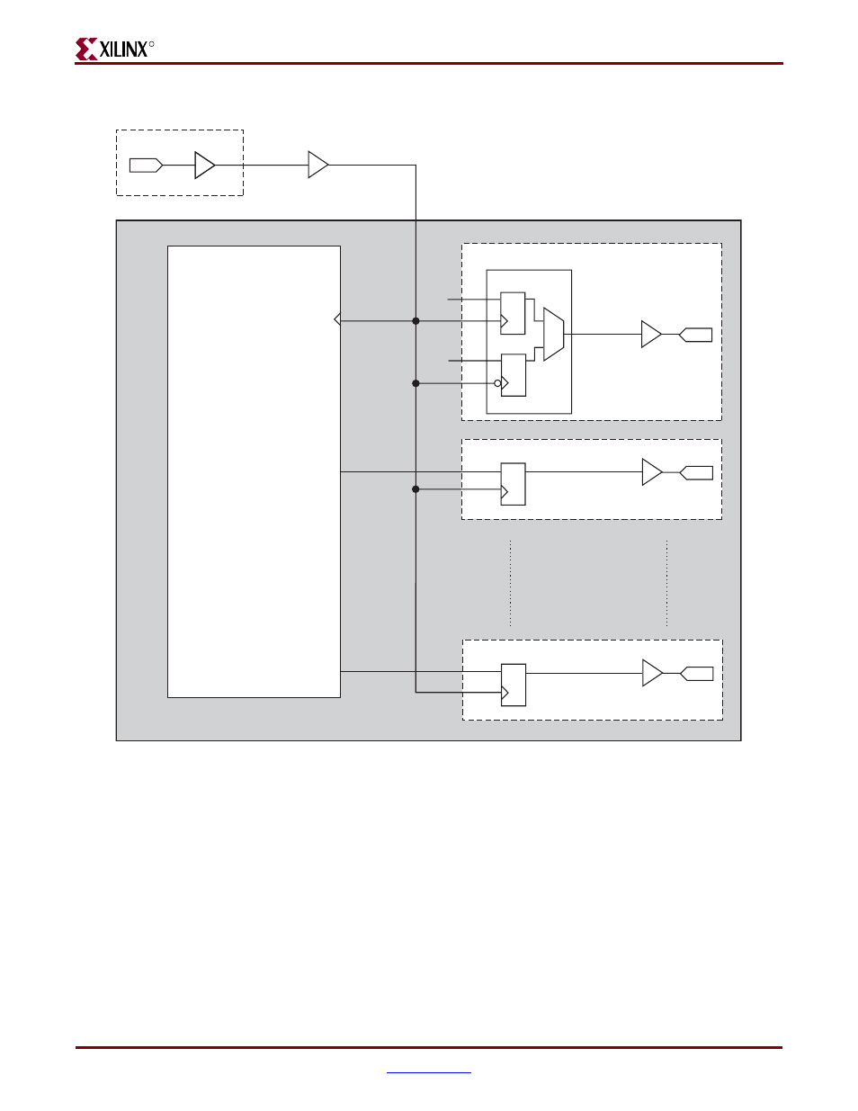
Figure 6-1:
Ten-Bit Interface Transmitter Logic
IPAD
IBUFG
IOB LOGIC
gtx_clk
gtx_clk_ibufg
(125 MHz)
BUFG
gtx_clk_bufg
pma_tx_clk
OBUF
FDDRRSE
IOB LOGIC
OPAD
D
Q
D
Q
pma_tx_clk_obuf
'0'
'1'
D
Q
tx_code_group[0]
OBUF
OPAD
tx_code_group_reg[0]
D
Q
tx_code_group[9]
OBUF
OPAD
tx_code_group_reg[9]
Ethernet 1000BASE-X PCS/PMA
or SGMII LogiCORE
tx_code_group_int[0]
tx_code_group_int[9]
gtx_clk
tx_code_group[0]
tx_code_group[9]
component_name_block (Block Level from example design)
