6 test signals, Table 3.6 test signals for lsi logic only, Test signals – Avago Technologies LSI53C320 User Manual
Page 41: Test signals for lsi logic only
Test Signals
3-7
Version 2.2
Copyright © 2003 by LSI Logic Corporation. All rights reserved.
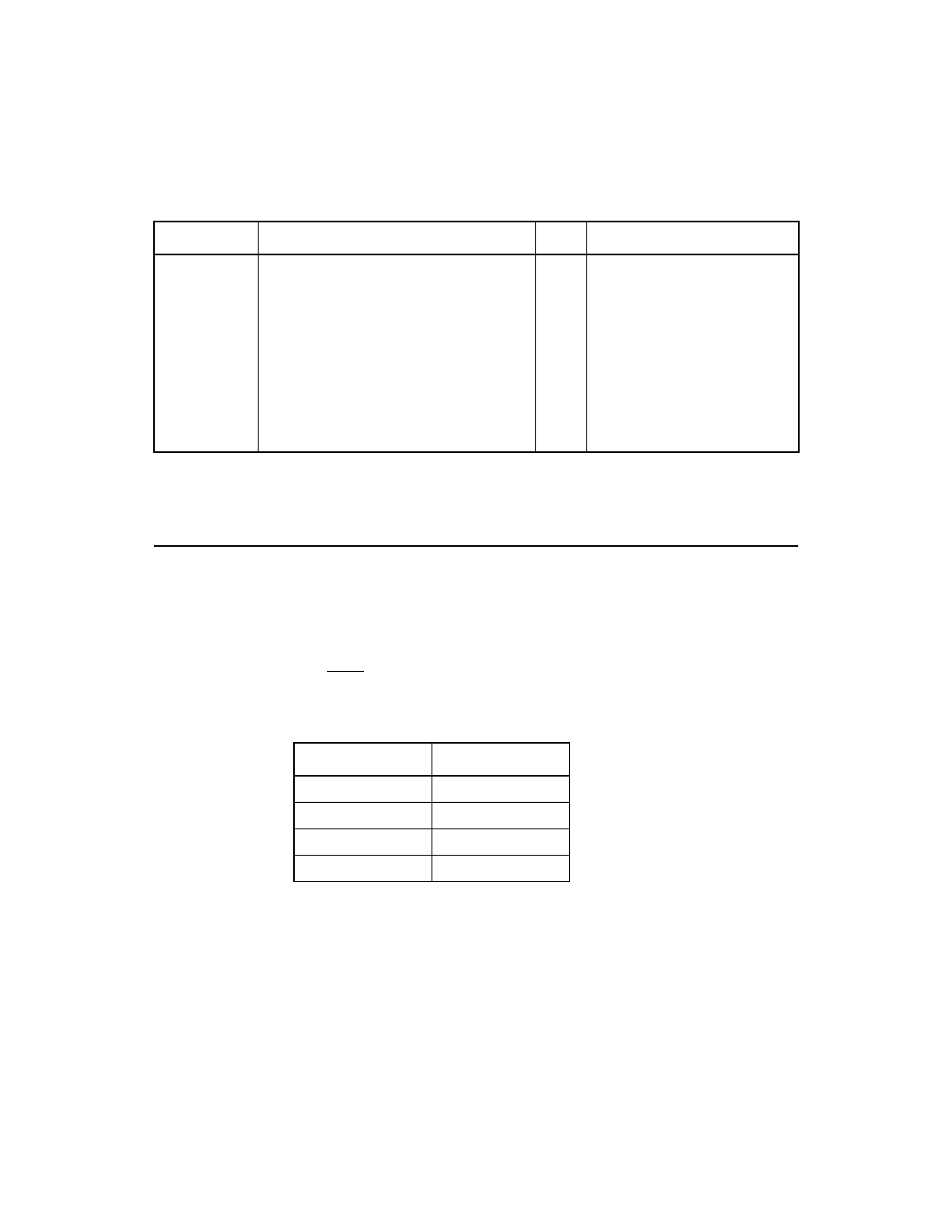
3.6 Test Signals
lists the LSI53C320 test signals and their associated ball
number. These test signals are for use by LSI Logic only.
Note:
Connect the tests signals to either test point or a header for
debugging purposes.
NC
A3, A5, A6, A10, B8, C4, C6, C9, C18, D5,
D7, D9, D12, D14, D16, E4, E17, G4,
G17, J4, J17, M4, M17, N18, P4, P17,
P18, P19, P20, R18, R19, R20, T4, T17,
T18, T19, T20, U5, U7, U9, U12, U14,
U16, U18, U19, U20, V3, V6, V7, V8, V9,
V10, V11, V12, V13, V14, V15, V16, V17,
V18, V19, V20, W6, W7, W8, W9, W10,
W11, W12, W13, W14, W15, W16, W17,
W18, W20, Y5, Y6, Y7, Y8, Y9, Y10, Y12,
Y13, Y14, Y15, Y16, Y17, Y18, Y19
N/A
No Connections.
1. VDD
SCSI
must be supplied with 3.3 V.
2. VDD
CORE
pins must be supplied 1.8 V.
3. VDD
IO
must be supplied with 3.3 V.
4. The VDD
IO
pin must always power down before the VDD
CORE
pin.
Table 3.5
Power and Ground Pins (Cont.)
Signal Name
Pin
Type
Description
Table 3.6
Test Signals for LSI Logic Only
Signal
Ball
TEST_3
A4
TEST_4
C5
TEST_5
B5
TEST_6
B4