4 serial eeprom signals, Table 3.4 serial eeprom signals, 5 power and ground signals – Avago Technologies LSI53C320 User Manual
Page 40: Table 3.5 power and ground pins (cont.), Serial eeprom signals, Power and ground signals, Power and ground pins
3-6
Signal Description
Version 2.2
Copyright © 2003 by LSI Logic Corporation. All rights reserved.
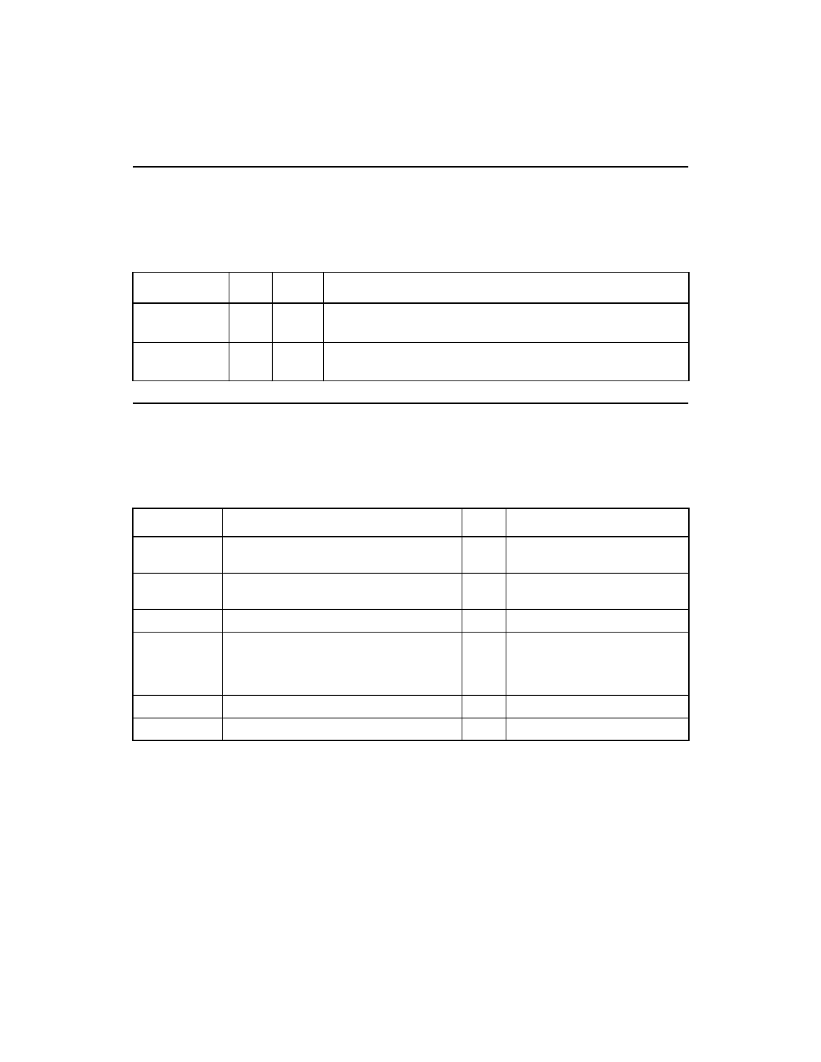
3.4 Serial EEPROM Signals
describes the serial EEPROM signals for the LSI53C320.
3.5 Power and Ground Signals
describes the power and ground signals for the LSI53C320.
Table 3.4
Serial EEPROM Signals
Signal Name
Pin
Type
Description
S_CLK
C7
O
The LSI53C320 uses the serial EEPROM clock signal to provide
the 50 kHz clock for downloading the serial EEPROM data.
S_DATA
B6
I/O
The LSI53C320 uses the serial EEPROM data signal to
download data from the serial EEPROM.
Table 3.5
Power and Ground Pins
Signal Name
Pin
Type
Description
VDD
SCSI
1
D6, D11, D15, F4, F17, K4, L17, R4, R17,
U6, U10, U15
I
Power supplies to the SCSI bus
I/O pins.
VDD
CORE
2
A2, B19, D10, K17, L4, U11, W2, W19
I
Power supplies to the CORE
logic.
VDD
IO
3, 4
C8
I
Power supplies to the I/O logic.
VSS
SCSI
A1, D4, D8, D13, D17, H4, H17, J9, J10,
J11, J12, K9, K10, K11, K12, L9, L10, L11,
L12, M9, M10, M11, M12, N4, N17, U4,
U8, U13, U17
I
Ground ring.
VSS
CORE
4
A20, B10, C3, K20, L1, Y1, Y11, Y20
I
Ground ring.
VSS
IO
B7
I
Ground ring.